IEC TS 62607-6-4:2016
(Main)Nanomanufacturing - Key control characteristics - Part 6-4: Graphene - Surface conductance measurement using resonant cavity
Nanomanufacturing - Key control characteristics - Part 6-4: Graphene - Surface conductance measurement using resonant cavity
IEC TS 62607-6-4:2016(E) establishes a method for determining the surface conductance of two-dimensional (2D) single-layer or multi-layer atomically thin nano-carbon graphene structures. These are synthesized by chemical vapour deposition (CVD), epitaxial growth on silicon carbide (SiC), obtained from reduced graphene oxide (rGO) or mechanically exfoliated from graphite. The measurements are made in an air filled standard R100 rectangular waveguide configuration, at one of the resonant frequency modes, typically at 7 GHz. Surface conductance measurement by resonant cavity involves monitoring the resonant frequency shift and change in the quality factor before and after insertion of the specimen into the cavity in a quantitative correlation with the specimen surface area. This measurement does not explicitly depend on the thickness of the nano-carbon layer. The thickness of the specimen does not need to be known, but it is assumed that the lateral dimension is uniform over the specimen area.
General Information
- Status
- Published
- Publication Date
- 27-Sep-2016
- Technical Committee
- TC 113 - Nanotechnology for electrotechnical products and systems
- Drafting Committee
- PT 62607-6-4 - TC 113/PT 62607-6-4
- Current Stage
- DELPUB - Deleted Publication
- Start Date
- 28-Feb-2024
- Completion Date
- 07-Apr-2022
Relations
- Effective Date
- 05-Sep-2023
Overview
IEC TS 62607-6-4:2016 is a Technical Specification published by the International Electrotechnical Commission (IEC) that defines a standardized method for measuring the surface conductance of two-dimensional (2D) single-layer or multi-layer graphene structures. It applies to graphene produced by various means such as chemical vapour deposition (CVD), epitaxial growth on silicon carbide (SiC), reduction of graphene oxide (rGO), and mechanical exfoliation from graphite.
The method specified in IEC TS 62607-6-4 uses a resonant cavity within a standard rectangular waveguide setup, typically operating around 7 GHz. The technique is non-contact and provides quantitative measurement of the surface conductance by analyzing changes in resonant frequency and quality factor when the graphene sample is placed inside the cavity. This standard ensures reproducible and accurate assessment of graphene’s key electrical property, supporting quality control, research, and industrial application in the field of nanomanufacturing.
Key Topics
- Surface Conductance Measurement: Defines a precise, non-contact approach to assess the ability of graphene layers to conduct electric current across their surface, using resonant cavity perturbation.
- Applicable Graphene Materials: Covers single-layer, bilayer, trilayer, and few-layer graphene, including chemically modified forms like graphene oxide and reduced graphene oxide.
- Measurement Setup: Utilizes an air-filled R100 (WR-90) rectangular waveguide and a vector network analyzer to monitor resonant frequency changes and quality factor before and after sample insertion.
- Sample Requirements: Assumes specimens have uniform lateral dimensions; thickness is not critical. Recommended substrate materials provide low dielectric permittivity and conductivity for minimal interference.
- Calibration and Accuracy: Describes calibration procedures for network analyzers and discusses measurement uncertainty, ensuring reliable and repeatable results.
Applications
The method outlined in IEC TS 62607-6-4:2016 is crucial to several domains within nanotechnology and materials science:
- Quality Control in Manufacturing: Enables consistent evaluation of graphene’s surface conductance during the production process, facilitating high-standard electronic and optoelectronic products.
- Research and Development: Provides researchers a standardized, accurate means of comparing electrical properties across graphene samples prepared by different methods or treatments.
- Device Fabrication: Assists in material selection for advanced devices such as high-speed electronics, sensors, transparent conductors, and flexible displays, where surface conductance is a critical performance metric.
- Comparative Material Analysis: Supports benchmarking of different synthesis routes, such as CVD, SiC epitaxy, or rGO, by offering a common measurement framework.
Related Standards
For comprehensive graphene characterization and alignment with best practices, the following standards are relevant:
- IEC 62607 Series: Other parts in this series address various key control characteristics for nanomanufactured materials.
- IEC 60153-2: Specifies requirements for hollow metallic waveguides, including those used in the resonant cavity setup.
- ISO/TS 80004-3: Provides foundational terminology for graphene and related nano-objects.
- General Graphene Characterization Standards: Often referenced in research and industry for structural, chemical, and electrical analysis of graphene and carbon nanomaterials.
Practical Value
Adopting IEC TS 62607-6-4:2016 ensures internationally recognized, reproducible measurement of graphene’s surface conductance-a key property underpinning its functional role in electronics and advanced materials. By standardizing methods and terminology, it facilitates collaboration, quality assurance, and innovation in nanomanufacturing and graphene technology.
Buy Documents
IEC TS 62607-6-4:2016 - Nanomanufacturing - Key control characteristics - Part 6-4: Graphene - Surface conductance measurement using resonant cavity
IEC TS 62607-6-4:2016 - Nanomanufacturing - Key control characteristics - Part 6-4: Graphene - Surface conductance measurement using resonant cavity Released:9/28/2016
Get Certified
Connect with accredited certification bodies for this standard

IMQ S.p.A. (Certification)
Italian electrical product certification.

SLG Prüf- und Zertifizierungs GmbH
German testing and certification body.

UL Solutions
Global safety science company with testing, inspection and certification.
Sponsored listings
Frequently Asked Questions
IEC TS 62607-6-4:2016 is a technical specification published by the International Electrotechnical Commission (IEC). Its full title is "Nanomanufacturing - Key control characteristics - Part 6-4: Graphene - Surface conductance measurement using resonant cavity". This standard covers: IEC TS 62607-6-4:2016(E) establishes a method for determining the surface conductance of two-dimensional (2D) single-layer or multi-layer atomically thin nano-carbon graphene structures. These are synthesized by chemical vapour deposition (CVD), epitaxial growth on silicon carbide (SiC), obtained from reduced graphene oxide (rGO) or mechanically exfoliated from graphite. The measurements are made in an air filled standard R100 rectangular waveguide configuration, at one of the resonant frequency modes, typically at 7 GHz. Surface conductance measurement by resonant cavity involves monitoring the resonant frequency shift and change in the quality factor before and after insertion of the specimen into the cavity in a quantitative correlation with the specimen surface area. This measurement does not explicitly depend on the thickness of the nano-carbon layer. The thickness of the specimen does not need to be known, but it is assumed that the lateral dimension is uniform over the specimen area.
IEC TS 62607-6-4:2016(E) establishes a method for determining the surface conductance of two-dimensional (2D) single-layer or multi-layer atomically thin nano-carbon graphene structures. These are synthesized by chemical vapour deposition (CVD), epitaxial growth on silicon carbide (SiC), obtained from reduced graphene oxide (rGO) or mechanically exfoliated from graphite. The measurements are made in an air filled standard R100 rectangular waveguide configuration, at one of the resonant frequency modes, typically at 7 GHz. Surface conductance measurement by resonant cavity involves monitoring the resonant frequency shift and change in the quality factor before and after insertion of the specimen into the cavity in a quantitative correlation with the specimen surface area. This measurement does not explicitly depend on the thickness of the nano-carbon layer. The thickness of the specimen does not need to be known, but it is assumed that the lateral dimension is uniform over the specimen area.
IEC TS 62607-6-4:2016 is classified under the following ICS (International Classification for Standards) categories: 07.120 - Nanotechnologies; 29.120.20 - Connecting devices. The ICS classification helps identify the subject area and facilitates finding related standards.
IEC TS 62607-6-4:2016 has the following relationships with other standards: It is inter standard links to IEC TS 62607-6-4:2024. Understanding these relationships helps ensure you are using the most current and applicable version of the standard.
IEC TS 62607-6-4:2016 is available in PDF format for immediate download after purchase. The document can be added to your cart and obtained through the secure checkout process. Digital delivery ensures instant access to the complete standard document.
Standards Content (Sample)
IEC TS 62607-6-4 ®
Edition 1.0 2016-09
TECHNICAL
SPECIFICATION
colour
inside
Nanomanufacturing – Key control characteristics –
Part 6-4: Graphene – Surface conductance measurement using resonant cavity
All rights reserved. Unless otherwise specified, no part of this publication may be reproduced or utilized in any form
or by any means, electronic or mechanical, including photocopying and microfilm, without permission in writing from
either IEC or IEC's member National Committee in the country of the requester. If you have any questions about IEC
copyright or have an enquiry about obtaining additional rights to this publication, please contact the address below or
your local IEC member National Committee for further information.
IEC Central Office Tel.: +41 22 919 02 11
3, rue de Varembé Fax: +41 22 919 03 00
CH-1211 Geneva 20 info@iec.ch
Switzerland www.iec.ch
About the IEC
The International Electrotechnical Commission (IEC) is the leading global organization that prepares and publishes
International Standards for all electrical, electronic and related technologies.
About IEC publications
The technical content of IEC publications is kept under constant review by the IEC. Please make sure that you have the
latest edition, a corrigenda or an amendment might have been published.
IEC Catalogue - webstore.iec.ch/catalogue Electropedia - www.electropedia.org
The stand-alone application for consulting the entire The world's leading online dictionary of electronic and
bibliographical information on IEC International Standards, electrical terms containing 20 000 terms and definitions in
Technical Specifications, Technical Reports and other English and French, with equivalent terms in 15 additional
documents. Available for PC, Mac OS, Android Tablets and languages. Also known as the International Electrotechnical
iPad. Vocabulary (IEV) online.
IEC publications search - www.iec.ch/searchpub IEC Glossary - std.iec.ch/glossary
The advanced search enables to find IEC publications by a 65 000 electrotechnical terminology entries in English and
variety of criteria (reference number, text, technical French extracted from the Terms and Definitions clause of
committee,…). It also gives information on projects, replaced IEC publications issued since 2002. Some entries have been
and withdrawn publications. collected from earlier publications of IEC TC 37, 77, 86 and
CISPR.
IEC Just Published - webstore.iec.ch/justpublished
Stay up to date on all new IEC publications. Just Published IEC Customer Service Centre - webstore.iec.ch/csc
details all new publications released. Available online and If you wish to give us your feedback on this publication or
also once a month by email. need further assistance, please contact the Customer Service
Centre: csc@iec.ch.
IEC TS 62607-6-4 ®
Edition 1.0 2016-09
TECHNICAL
SPECIFICATION
colour
inside
Nanomanufacturing – Key control characteristics –
Part 6-4: Graphene – Surface conductance measurement using resonant cavity
INTERNATIONAL
ELECTROTECHNICAL
COMMISSION
ICS 07.120 ISBN 978-2-8322-3667-3
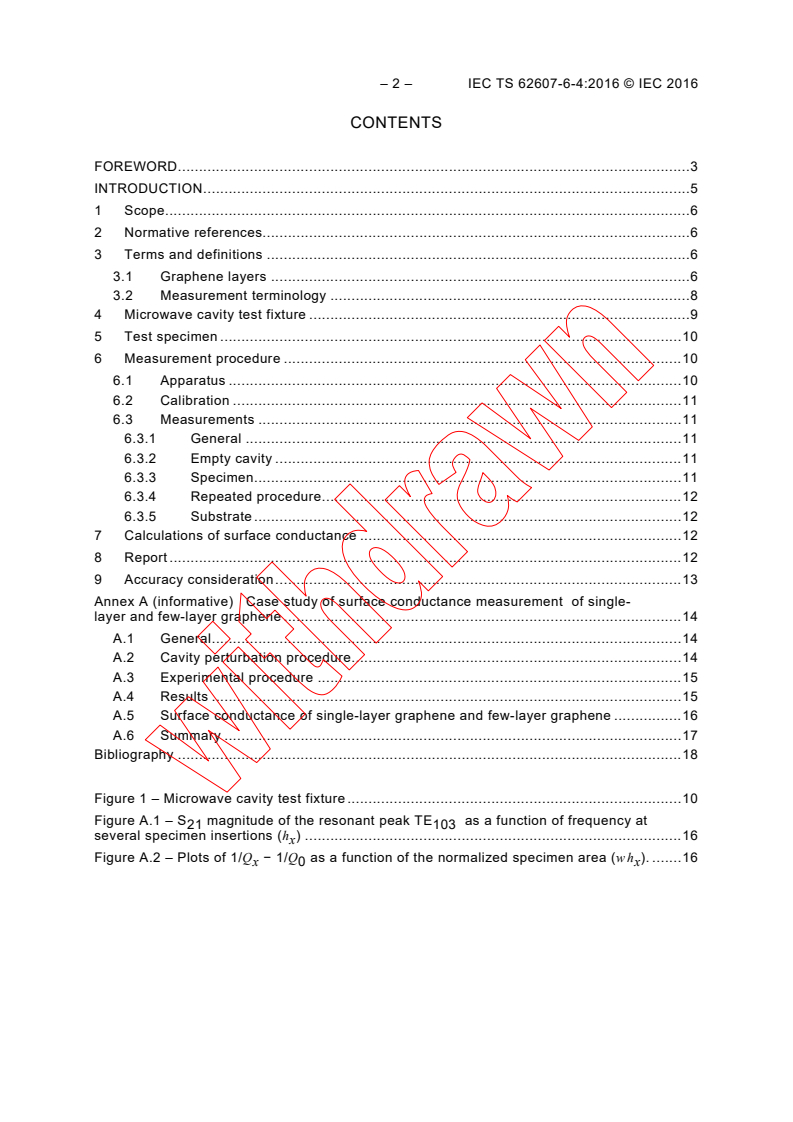
– 2 – IEC TS 62607-6-4:2016 © IEC 2016
CONTENTS
FOREWORD . 3
INTRODUCTION . 5
1 Scope . 6
2 Normative references. 6
3 Terms and definitions . 6
3.1 Graphene layers . 6
3.2 Measurement terminology . 8
4 Microwave cavity test fixture . 9
5 Test specimen . 10
6 Measurement procedure . 10
6.1 Apparatus . 10
6.2 Calibration . 11
6.3 Measurements . 11
6.3.1 General . 11
6.3.2 Empty cavity . 11
6.3.3 Specimen. 11
6.3.4 Repeated procedure . 12
6.3.5 Substrate . 12
7 Calculations of surface conductance . 12
8 Report . 12
9 Accuracy consideration . 13
Annex A (informative) Case study of surface conductance measurement of single-
layer and few-layer graphene . 14
A.1 General . 14
A.2 Cavity perturbation procedure . 14
A.3 Experimental procedure . 15
A.4 Results . 15
A.5 Surface conductance of single-layer graphene and few-layer graphene . 16
A.6 Summary . 17
Bibliography . 18
Figure 1 – Microwave cavity test fixture . 10
Figure A.1 – S magnitude of the resonant peak TE as a function of frequency at
21 103
several specimen insertions (h ) . 16
x
Figure A.2 – Plots of 1/Q − 1/Q as a function of the normalized specimen area (w h ). . 16
x 0 x
INTERNATIONAL ELECTROTECHNICAL COMMISSION
____________
NANOMANUFACTURING –
KEY CONTROL CHARACTERISTICS –
Part 6-4: Graphene – Surface conductance
measurement using resonant cavity
FOREWORD
1) The International Electrotechnical Commission (IEC) is a worldwide organization for standardization comprising
all national electrotechnical committees (IEC National Committees). The object of IEC is to promote
international co-operation on all questions concerning standardization in the electrical and electronic fields. To
this end and in addition to other activities, IEC publishes International Standards, Technical Specifications,
Technical Reports, Publicly Available Specifications (PAS) and Guides (hereafter referred to as “IEC
Publication(s)”). Their preparation is entrusted to technical committees; any IEC National Committee interested
in the subject dealt with may participate in this preparatory work. International, governmental and non-
governmental organizations liaising with the IEC also participate in this preparation. IEC collaborates closely
with the International Organization for Standardization (ISO) in accordance with conditions determined by
agreement between the two organizations.
2) The formal decisions or agreements of IEC on technical matters express, as nearly as possible, an international
consensus of opinion on the relevant subjects since each technical committee has representation from all
interested IEC National Committees.
3) IEC Publications have the form of recommendations for international use and are accepted by IEC National
Committees in that sense. While all reasonable efforts are made to ensure that the technical content of IEC
Publications is accurate, IEC cannot be held responsible for the way in which they are used or for any
misinterpretation by any end user.
4) In order to promote international uniformity, IEC National Committees undertake to apply IEC Publications
transparently to the maximum extent possible in their national and regional publications. Any divergence
between any IEC Publication and the corresponding national or regional publication shall be clearly indicated in
the latter.
5) IEC itself does not provide any attestation of conformity. Independent certification bodies provide conformity
assessment services and, in some areas, access to IEC marks of conformity. IEC is not responsible for any
services carried out by independent certification bodies.
6) All users should ensure that they have the latest edition of this publication.
7) No liability shall attach to IEC or its directors, employees, servants or agents including individual experts and
members of its technical committees and IEC National Committees for any personal injury, property damage or
other damage of any nature whatsoever, whether direct or indirect, or for costs (including legal fees) and
expenses arising out of the publication, use of, or reliance upon, this IEC Publication or any other IEC
Publications.
8) Attention is drawn to the Normative references cited in this publication. Use of the referenced publications is
indispensable for the correct application of this publication.
9) Attention is drawn to the possibility that some of the elements of this IEC Publication may be the subject of
patent rights. IEC shall not be held responsible for identifying any or all such patent rights.
The main task of IEC technical committees is to prepare International Standards. In
exceptional circumstances, a technical committee may propose the publication of a Technical
Specification when
• the required support cannot be obtained for the publication of an International Standard,
despite repeated efforts, or
• the subject is still under technical development or where, for any other reason, there is the
future but no immediate possibility of an agreement on an International Standard.
Technical Specifications are subject to review within three years of publication to decide
whether they can be transformed into International Standards.
IEC TS 62607-6-4, which is a Technical Specification, has been prepared by IEC technical
committee 113: Nanotechnology for electrotechnical products and systems.
– 4 – IEC TS 62607-6-4:2016 © IEC 2016
The text of this Technical Specification is based on the following documents:
Enquiry draft Report on voting
113/295/DTS 113/324/RVC
Full information on the voting for the approval of this Technical Specification can be found in
the report on voting indicated in the above table.
This document has been drafted in accordance with the ISO/IEC Directives, Part 2.
A list of all parts in the IEC 62607 series, published under the general title
Nanomanufacturing – Key control characteristics, can be found on the IEC website.
The committee has decided that the contents of this document will remain unchanged until the
stability date indicated on the IEC website under "http://webstore.iec.ch" in the data related to
the specific document. At this date, the document will be
• transformed into an International Standard,
• reconfirmed,
• withdrawn,
• replaced by a revised edition, or
• amended.
A bilingual version of this publication may be issued at a later date.
IMPORTANT – The 'colour inside' logo on the cover page of this publication indicates
that it contains colours which are considered to be useful for the correct
understanding of its contents. Users should therefore print this document using a
colour printer.
INTRODUCTION
The microwave resonant cavity test method for surface conductance is non-contact, fast,
sensitive and accurate. It is well suited for standards, research and development (R&D), and
for quality control in the manufacturing of two-dimensional (2D) nano-carbon materials. These
sheet-like or flake-like carbon forms can be assembled into atomically-thin monolayer or
multilayer graphene materials, which can be stacked, folded, crumpled or pillared into a
variety of nano-carbon architectures with the lateral dimension limited to a few tenths of a
nanometre. Many of these materials are new and exhibit extraordinary physical and electrical
properties such as optical transparency, anisotropic heat diffusivity and charge transport that
are of significant interest to science, technology and commercial applications [1, 2] .
Depending on particular morphologies, density of states and structural perfection, the surface
−4
conductance of these materials may vary from 1 S to about 10 S. Conventional direct
current (DC) surface conductance measurement techniques require a complex test vehicle
and interconnections for making electrical contacts, which affect and alter the measurement,
making it difficult to decouple the intrinsic properties of the material.
In comparison, the resonant cavity measurement method is fast and non-contact. Thus, it is
well suited for use in R&D and manufacturing environments where the surface conductance is
a critical functional parameter. Moreover, it can be employed to measure electrical
characteristics of other nano-size structures.
___________
Numbers in square brackets refer to the Bibliography
– 6 – IEC TS 62607-6-4:2016 © IEC 2016
NANOMANUFACTURING –
KEY CONTROL CHARACTERISTICS –
Part 6-4: Graphene – Surface conductance
measurement using resonant cavity
1 Scope
This part of IEC 62607 establishes a method for determining the surface conductance of two-
dimensional (2D) single-layer or multi-layer atomically thin nano-carbon graphene structures.
These are synthesized by chemical vapour deposition (CVD), epitaxial growth on silicon
carbide (SiC), obtained from reduced graphene oxide (rGO) or mechanically exfoliated from
graphite [3]. The measurements are made in an air filled standard R100 rectangular
waveguide configuration, at one of the resonant frequency modes, typically at 7 GHz [4].
Surface conductance measurement by resonant cavity involves monitoring the resonant
frequency shift and change in the quality factor before and after insertion of the specimen into
the cavity in a quantitative correlation with the specimen surface area. This measurement
does not explicitly depend on the thickness of the nano-carbon layer. The thickness of the
specimen does not need to be known, but it is assumed that the lateral dimension is uniform
over the specimen area.
2 Normative references
The following documents are referred to in the text in such a way that some or all of their
content constitutes requirements of this document. For dated references, only the edition
cited applies. For undated references, the latest edition of the referenced document (including
any amendments) applies.
IEC 60153-2, Hollow metallic waveguides – Part 2: Relevant specifications for ordinary
rectangular waveguides
3 Terms and definitions
For the purposes of this document, the terms and definitions given in IEC 60153-2 and the
following apply.
ISO and IEC maintain terminological databases for use in standardization at the following
addresses:
• IEC Electropedia: available at http://www.electropedia.org/
• ISO Online browsing platform: available at http://www.iso.org/obp
3.1 Graphene layers
3.1.1
graphene
single-layer graphene
1LG
single layer of carbon atoms with sp -electronic hybridization bound to three neighbours in a
honeycomb structure
Note 1 to entry: It is an important building block of many carbon nano-objects.
[SOURCE: ISO/TS 80004-3:2010, 2.11, modified.]
3.1.2
bilayer graphene
2LG
two-dimensional material consisting of two well-defined stacked graphene layers
Note 1 to entry: If the stacking registry is known it can be specified separately, for example as "Bernal stacked
bilayer graphene”.
3.1.3
trilayer graphene
3LG
two-dimensional material consisting of three well-defined stacked graphene layers
Note 1 to entry: If the stacking registry is known it can be specified separately, for example as "Bernal stacked
trilayer graphene" or "twisted trilayer graphene”.
3.1.4
few-layer graphene
FLG
two-dimensional material consisting of three to ten well-defined stacked graphene layers
3.1.5
nanoplate
nano-object with one external dimension in the nanoscale and the other two external
dimensions significantly larger
[SOURCE: ISO/TS 80004-2:2015, 4.6]
3.1.6
nanosheet
nanoplate with extended lateral dimensions
3.1.7
graphene oxide
GO
chemically modified graphene prepared by oxidation and exfoliation of graphite that is
accompanied by extensive oxidative modification of the basal plane
Note 1 to entry: Graphene oxide is a single material with a high oxygen content, typically characterized by C/O
atomic ratios less than 3.0 and typically closer to 2.0.
3.1.8
reduced graphene oxide
rGO
graphene oxide that has been processed to reduce its oxygen content
Note 1 to entry: This can be produced by chemical, thermal, microwave, photo-chemical, photo-thermal or
microbial/bacterial methods or by exfoliating reduced graphite oxide.
Note 2 to entry: If graphene oxide was fully reduced then graphene would be the product, however in practice
3 2
some oxygen containing functional groups will remain and not all sp bonds will return back to sp configuration.
Different reducing agents will lead to different carbon to oxygen ratios and different chemical compositions in
reduced graphene oxide
– 8 – IEC TS 62607-6-4:2016 © IEC 2016
3.1.9
graphene material
nanomaterial based on graphene
Note 1 to entry: Examples of graphene material are multilayered graphene (less than about 10 layers), chemically
modified forms (GO, rGO), and materials made via another precursor material or process such as chemical vapour
deposition (CVD) [3].
3.2 Measurement terminology
3.2.1
s
s
surface conductance
characteristic physical property of two-dimensional materials describing the ability to conduct
electric current
Note 1 to entry The SI unit of measure of s is siemens (S). In the trade and industrial literature, however,
s
siemens per square (S/square) is commonly used when referring to surface conductance. This is to avoid confusion
between surface conductance and electric conductance (G), which share the same unit of measure:
G = I/U = s (w/l).
s
Note 2 to entry: The surface conductance (s ) can be obtained by normalizing conductance G to the specimen
s
width (w) and length (l).
3.2.2
G
electric conductance
measure of how easily electric current flows along a certain path
Note 1 to entry: The SI unit of electric conductance is siemens (S).
3.2.3
s
v
volume conductivity
characteristic physical property of three-dimensional materials describing the ability to
conduct electric current
Note 1 to entry: The volume conductivity can be obtained by dividing the surface conductance by the conductor
thickness (t):
s = s /t.
v s
The unit of measure of s is siemens per metre (S/m).
v
3.2.4
ρ
s
surface resistance
sheet resistance
reciprocal of s
s
Note 1 to entry: ρ is a characteristic property of two-dimensional materials. The SI unit of measure of ρ is ohm
s s
(Ω). In the trade and industrial literature, however, ohm per square (Ω/square) is commonly used when referring to
surface resistance or sheet resistance.
3.2.5
microwave cavity
radio frequency cavity
RF cavity
resonator consisting of a closed metal structure that confines electromagnetic fields in the
microwave region of the spectrum
Note 1 to entry: The structure can be filled with air or other dielectric material. A cavity acts similarly to a
resonant circuit with extremely low loss at its frequency of operation. Microwave cavities are typically made from
closed (or short-circuited) sections of a waveguide. Every cavity has numerous resonant frequencies (f ) that
r
correspond to electromagnetic field modes satisfying the necessary boundary conditions, i.e. the cavity length is an
integer multiple of half-wavelength at resonance.
3.2.6
Q
quality factor
dimension-less parameter describing the ratio of energy stored in the resonant circuit to time-
averaged power loss of the cavity, or equivalently, a resonator's half power bandwidth, (∆f)
relative to the resonant frequency (f ):
r
Q = f /∆f
r
3.2.7
S
ij
microwave scattering parameters
S-parameters
factors that quantify how RF energy propagates through a microwave multi-port network.
Note 1 to entry: Subscript (i) indicates the detecting port. Subscript (j) refers to the sourcing (input) port.
Accordingly, S quantifies microwave energy th
...
IEC TS 62607-6-4 ®
Edition 1.0 2016-09
TECHNICAL
SPECIFICATION
colour
inside
Nanomanufacturing – Key control characteristics –
Part 6-4: Graphene – Surface conductance measurement using resonant cavity
All rights reserved. Unless otherwise specified, no part of this publication may be reproduced or utilized in any form
or by any means, electronic or mechanical, including photocopying and microfilm, without permission in writing from
either IEC or IEC's member National Committee in the country of the requester. If you have any questions about IEC
copyright or have an enquiry about obtaining additional rights to this publication, please contact the address below or
your local IEC member National Committee for further information.
IEC Central Office Tel.: +41 22 919 02 11
3, rue de Varembé Fax: +41 22 919 03 00
CH-1211 Geneva 20 info@iec.ch
Switzerland www.iec.ch
About the IEC
The International Electrotechnical Commission (IEC) is the leading global organization that prepares and publishes
International Standards for all electrical, electronic and related technologies.
About IEC publications
The technical content of IEC publications is kept under constant review by the IEC. Please make sure that you have the
latest edition, a corrigenda or an amendment might have been published.
IEC Catalogue - webstore.iec.ch/catalogue Electropedia - www.electropedia.org
The stand-alone application for consulting the entire The world's leading online dictionary of electronic and
bibliographical information on IEC International Standards, electrical terms containing 20 000 terms and definitions in
Technical Specifications, Technical Reports and other English and French, with equivalent terms in 15 additional
documents. Available for PC, Mac OS, Android Tablets and languages. Also known as the International Electrotechnical
iPad. Vocabulary (IEV) online.
IEC publications search - www.iec.ch/searchpub IEC Glossary - std.iec.ch/glossary
The advanced search enables to find IEC publications by a 65 000 electrotechnical terminology entries in English and
variety of criteria (reference number, text, technical French extracted from the Terms and Definitions clause of
committee,…). It also gives information on projects, replaced IEC publications issued since 2002. Some entries have been
and withdrawn publications. collected from earlier publications of IEC TC 37, 77, 86 and
CISPR.
IEC Just Published - webstore.iec.ch/justpublished
Stay up to date on all new IEC publications. Just Published IEC Customer Service Centre - webstore.iec.ch/csc
details all new publications released. Available online and If you wish to give us your feedback on this publication or
also once a month by email. need further assistance, please contact the Customer Service
Centre: csc@iec.ch.
IEC TS 62607-6-4 ®
Edition 1.0 2016-09
TECHNICAL
SPECIFICATION
colour
inside
Nanomanufacturing – Key control characteristics –
Part 6-4: Graphene – Surface conductance measurement using resonant cavity
INTERNATIONAL
ELECTROTECHNICAL
COMMISSION
ICS 07.120 ISBN 978-2-8322-3667-3
– 2 – IEC TS 62607-6-4:2016 © IEC 2016
CONTENTS
FOREWORD . 3
INTRODUCTION . 5
1 Scope . 6
2 Normative references. 6
3 Terms and definitions . 6
3.1 Graphene layers . 6
3.2 Measurement terminology . 8
4 Microwave cavity test fixture . 9
5 Test specimen . 10
6 Measurement procedure . 10
6.1 Apparatus . 10
6.2 Calibration . 11
6.3 Measurements . 11
6.3.1 General . 11
6.3.2 Empty cavity . 11
6.3.3 Specimen. 11
6.3.4 Repeated procedure . 12
6.3.5 Substrate . 12
7 Calculations of surface conductance . 12
8 Report . 12
9 Accuracy consideration . 13
Annex A (informative) Case study of surface conductance measurement of single-
layer and few-layer graphene . 14
A.1 General . 14
A.2 Cavity perturbation procedure . 14
A.3 Experimental procedure . 15
A.4 Results . 15
A.5 Surface conductance of single-layer graphene and few-layer graphene . 16
A.6 Summary . 17
Bibliography . 18
Figure 1 – Microwave cavity test fixture . 10
Figure A.1 – S magnitude of the resonant peak TE as a function of frequency at
21 103
several specimen insertions (h ) . 16
x
Figure A.2 – Plots of 1/Q − 1/Q as a function of the normalized specimen area (w h ). . 16
x 0 x
INTERNATIONAL ELECTROTECHNICAL COMMISSION
____________
NANOMANUFACTURING –
KEY CONTROL CHARACTERISTICS –
Part 6-4: Graphene – Surface conductance
measurement using resonant cavity
FOREWORD
1) The International Electrotechnical Commission (IEC) is a worldwide organization for standardization comprising
all national electrotechnical committees (IEC National Committees). The object of IEC is to promote
international co-operation on all questions concerning standardization in the electrical and electronic fields. To
this end and in addition to other activities, IEC publishes International Standards, Technical Specifications,
Technical Reports, Publicly Available Specifications (PAS) and Guides (hereafter referred to as “IEC
Publication(s)”). Their preparation is entrusted to technical committees; any IEC National Committee interested
in the subject dealt with may participate in this preparatory work. International, governmental and non-
governmental organizations liaising with the IEC also participate in this preparation. IEC collaborates closely
with the International Organization for Standardization (ISO) in accordance with conditions determined by
agreement between the two organizations.
2) The formal decisions or agreements of IEC on technical matters express, as nearly as possible, an international
consensus of opinion on the relevant subjects since each technical committee has representation from all
interested IEC National Committees.
3) IEC Publications have the form of recommendations for international use and are accepted by IEC National
Committees in that sense. While all reasonable efforts are made to ensure that the technical content of IEC
Publications is accurate, IEC cannot be held responsible for the way in which they are used or for any
misinterpretation by any end user.
4) In order to promote international uniformity, IEC National Committees undertake to apply IEC Publications
transparently to the maximum extent possible in their national and regional publications. Any divergence
between any IEC Publication and the corresponding national or regional publication shall be clearly indicated in
the latter.
5) IEC itself does not provide any attestation of conformity. Independent certification bodies provide conformity
assessment services and, in some areas, access to IEC marks of conformity. IEC is not responsible for any
services carried out by independent certification bodies.
6) All users should ensure that they have the latest edition of this publication.
7) No liability shall attach to IEC or its directors, employees, servants or agents including individual experts and
members of its technical committees and IEC National Committees for any personal injury, property damage or
other damage of any nature whatsoever, whether direct or indirect, or for costs (including legal fees) and
expenses arising out of the publication, use of, or reliance upon, this IEC Publication or any other IEC
Publications.
8) Attention is drawn to the Normative references cited in this publication. Use of the referenced publications is
indispensable for the correct application of this publication.
9) Attention is drawn to the possibility that some of the elements of this IEC Publication may be the subject of
patent rights. IEC shall not be held responsible for identifying any or all such patent rights.
The main task of IEC technical committees is to prepare International Standards. In
exceptional circumstances, a technical committee may propose the publication of a Technical
Specification when
• the required support cannot be obtained for the publication of an International Standard,
despite repeated efforts, or
• the subject is still under technical development or where, for any other reason, there is the
future but no immediate possibility of an agreement on an International Standard.
Technical Specifications are subject to review within three years of publication to decide
whether they can be transformed into International Standards.
IEC TS 62607-6-4, which is a Technical Specification, has been prepared by IEC technical
committee 113: Nanotechnology for electrotechnical products and systems.
– 4 – IEC TS 62607-6-4:2016 © IEC 2016
The text of this Technical Specification is based on the following documents:
Enquiry draft Report on voting
113/295/DTS 113/324/RVC
Full information on the voting for the approval of this Technical Specification can be found in
the report on voting indicated in the above table.
This document has been drafted in accordance with the ISO/IEC Directives, Part 2.
A list of all parts in the IEC 62607 series, published under the general title
Nanomanufacturing – Key control characteristics, can be found on the IEC website.
The committee has decided that the contents of this document will remain unchanged until the
stability date indicated on the IEC website under "http://webstore.iec.ch" in the data related to
the specific document. At this date, the document will be
• transformed into an International Standard,
• reconfirmed,
• withdrawn,
• replaced by a revised edition, or
• amended.
A bilingual version of this publication may be issued at a later date.
IMPORTANT – The 'colour inside' logo on the cover page of this publication indicates
that it contains colours which are considered to be useful for the correct
understanding of its contents. Users should therefore print this document using a
colour printer.
INTRODUCTION
The microwave resonant cavity test method for surface conductance is non-contact, fast,
sensitive and accurate. It is well suited for standards, research and development (R&D), and
for quality control in the manufacturing of two-dimensional (2D) nano-carbon materials. These
sheet-like or flake-like carbon forms can be assembled into atomically-thin monolayer or
multilayer graphene materials, which can be stacked, folded, crumpled or pillared into a
variety of nano-carbon architectures with the lateral dimension limited to a few tenths of a
nanometre. Many of these materials are new and exhibit extraordinary physical and electrical
properties such as optical transparency, anisotropic heat diffusivity and charge transport that
are of significant interest to science, technology and commercial applications [1, 2] .
Depending on particular morphologies, density of states and structural perfection, the surface
−4
conductance of these materials may vary from 1 S to about 10 S. Conventional direct
current (DC) surface conductance measurement techniques require a complex test vehicle
and interconnections for making electrical contacts, which affect and alter the measurement,
making it difficult to decouple the intrinsic properties of the material.
In comparison, the resonant cavity measurement method is fast and non-contact. Thus, it is
well suited for use in R&D and manufacturing environments where the surface conductance is
a critical functional parameter. Moreover, it can be employed to measure electrical
characteristics of other nano-size structures.
___________
Numbers in square brackets refer to the Bibliography
– 6 – IEC TS 62607-6-4:2016 © IEC 2016
NANOMANUFACTURING –
KEY CONTROL CHARACTERISTICS –
Part 6-4: Graphene – Surface conductance
measurement using resonant cavity
1 Scope
This part of IEC 62607 establishes a method for determining the surface conductance of two-
dimensional (2D) single-layer or multi-layer atomically thin nano-carbon graphene structures.
These are synthesized by chemical vapour deposition (CVD), epitaxial growth on silicon
carbide (SiC), obtained from reduced graphene oxide (rGO) or mechanically exfoliated from
graphite [3]. The measurements are made in an air filled standard R100 rectangular
waveguide configuration, at one of the resonant frequency modes, typically at 7 GHz [4].
Surface conductance measurement by resonant cavity involves monitoring the resonant
frequency shift and change in the quality factor before and after insertion of the specimen into
the cavity in a quantitative correlation with the specimen surface area. This measurement
does not explicitly depend on the thickness of the nano-carbon layer. The thickness of the
specimen does not need to be known, but it is assumed that the lateral dimension is uniform
over the specimen area.
2 Normative references
The following documents are referred to in the text in such a way that some or all of their
content constitutes requirements of this document. For dated references, only the edition
cited applies. For undated references, the latest edition of the referenced document (including
any amendments) applies.
IEC 60153-2, Hollow metallic waveguides – Part 2: Relevant specifications for ordinary
rectangular waveguides
3 Terms and definitions
For the purposes of this document, the terms and definitions given in IEC 60153-2 and the
following apply.
ISO and IEC maintain terminological databases for use in standardization at the following
addresses:
• IEC Electropedia: available at http://www.electropedia.org/
• ISO Online browsing platform: available at http://www.iso.org/obp
3.1 Graphene layers
3.1.1
graphene
single-layer graphene
1LG
single layer of carbon atoms with sp -electronic hybridization bound to three neighbours in a
honeycomb structure
Note 1 to entry: It is an important building block of many carbon nano-objects.
[SOURCE: ISO/TS 80004-3:2010, 2.11, modified.]
3.1.2
bilayer graphene
2LG
two-dimensional material consisting of two well-defined stacked graphene layers
Note 1 to entry: If the stacking registry is known it can be specified separately, for example as "Bernal stacked
bilayer graphene”.
3.1.3
trilayer graphene
3LG
two-dimensional material consisting of three well-defined stacked graphene layers
Note 1 to entry: If the stacking registry is known it can be specified separately, for example as "Bernal stacked
trilayer graphene" or "twisted trilayer graphene”.
3.1.4
few-layer graphene
FLG
two-dimensional material consisting of three to ten well-defined stacked graphene layers
3.1.5
nanoplate
nano-object with one external dimension in the nanoscale and the other two external
dimensions significantly larger
[SOURCE: ISO/TS 80004-2:2015, 4.6]
3.1.6
nanosheet
nanoplate with extended lateral dimensions
3.1.7
graphene oxide
GO
chemically modified graphene prepared by oxidation and exfoliation of graphite that is
accompanied by extensive oxidative modification of the basal plane
Note 1 to entry: Graphene oxide is a single material with a high oxygen content, typically characterized by C/O
atomic ratios less than 3.0 and typically closer to 2.0.
3.1.8
reduced graphene oxide
rGO
graphene oxide that has been processed to reduce its oxygen content
Note 1 to entry: This can be produced by chemical, thermal, microwave, photo-chemical, photo-thermal or
microbial/bacterial methods or by exfoliating reduced graphite oxide.
Note 2 to entry: If graphene oxide was fully reduced then graphene would be the product, however in practice
3 2
some oxygen containing functional groups will remain and not all sp bonds will return back to sp configuration.
Different reducing agents will lead to different carbon to oxygen ratios and different chemical compositions in
reduced graphene oxide
– 8 – IEC TS 62607-6-4:2016 © IEC 2016
3.1.9
graphene material
nanomaterial based on graphene
Note 1 to entry: Examples of graphene material are multilayered graphene (less than about 10 layers), chemically
modified forms (GO, rGO), and materials made via another precursor material or process such as chemical vapour
deposition (CVD) [3].
3.2 Measurement terminology
3.2.1
s
s
surface conductance
characteristic physical property of two-dimensional materials describing the ability to conduct
electric current
Note 1 to entry The SI unit of measure of s is siemens (S). In the trade and industrial literature, however,
s
siemens per square (S/square) is commonly used when referring to surface conductance. This is to avoid confusion
between surface conductance and electric conductance (G), which share the same unit of measure:
G = I/U = s (w/l).
s
Note 2 to entry: The surface conductance (s ) can be obtained by normalizing conductance G to the specimen
s
width (w) and length (l).
3.2.2
G
electric conductance
measure of how easily electric current flows along a certain path
Note 1 to entry: The SI unit of electric conductance is siemens (S).
3.2.3
s
v
volume conductivity
characteristic physical property of three-dimensional materials describing the ability to
conduct electric current
Note 1 to entry: The volume conductivity can be obtained by dividing the surface conductance by the conductor
thickness (t):
s = s /t.
v s
The unit of measure of s is siemens per metre (S/m).
v
3.2.4
ρ
s
surface resistance
sheet resistance
reciprocal of s
s
Note 1 to entry: ρ is a characteristic property of two-dimensional materials. The SI unit of measure of ρ is ohm
s s
(Ω). In the trade and industrial literature, however, ohm per square (Ω/square) is commonly used when referring to
surface resistance or sheet resistance.
3.2.5
microwave cavity
radio frequency cavity
RF cavity
resonator consisting of a closed metal structure that confines electromagnetic fields in the
microwave region of the spectrum
Note 1 to entry: The structure can be filled with air or other dielectric material. A cavity acts similarly to a
resonant circuit with extremely low loss at its frequency of operation. Microwave cavities are typically made from
closed (or short-circuited) sections of a waveguide. Every cavity has numerous resonant frequencies (f ) that
r
correspond to electromagnetic field modes satisfying the necessary boundary conditions, i.e. the cavity length is an
integer multiple of half-wavelength at resonance.
3.2.6
Q
quality factor
dimension-less parameter describing the ratio of energy stored in the resonant circuit to time-
averaged power loss of the cavity, or equivalently, a resonator's half power bandwidth, (∆f)
relative to the resonant frequency (f ):
r
Q = f /∆f
r
3.2.7
S
ij
microwave scattering parameters
S-parameters
factors that quantify how RF energy propagates through a microwave multi-port network.
Note 1 to entry: Subscript (i) indicates the detecting port. Subscript (j) refers to the sourcing (input) port.
Accordingly, S quant
...
Questions, Comments and Discussion
Ask us and Technical Secretary will try to provide an answer. You can facilitate discussion about the standard in here.
Loading comments...