IEC TS 62607-6-9:2022
(Main)Nanomanufacturing - Key control characteristics - Part 6-9: Graphene-based material - Sheet resistance: Eddy current method
Nanomanufacturing - Key control characteristics - Part 6-9: Graphene-based material - Sheet resistance: Eddy current method
IEC 62607-6-9:2022(EN) establishes a standardized method to determine the key control characteristic
• sheet resistance
for films of graphene-based materials by
• eddy current method.
General Information
- Status
- Published
- Publication Date
- 07-Feb-2022
- Technical Committee
- TC 113 - Nanotechnology for electrotechnical products and systems
- Drafting Committee
- PT 62607-6-9 - TC 113/PT 62607-6-9
- Current Stage
- PPUB - Publication issued
- Start Date
- 08-Feb-2022
- Completion Date
- 03-Mar-2022
Overview
IEC TS 62607-6-9:2022 - Nanomanufacturing – Key control characteristics – Part 6-9: Graphene-based material – Sheet resistance: Eddy current method (Edition 1.0, 2022) is an IEC Technical Specification from TC 113 that defines a standardized, non-contact method to measure sheet resistance of graphene-based films using an eddy current technique. The method uses a coil-generated alternating electromagnetic field to induce eddy currents in the conductive graphene layer; the resulting secondary field is measured and correlated to sheet resistance. The specification targets contactless electrical characterization and quality control of large-area graphene layers on non-conductive substrates.
Key topics and technical requirements
- Measurement principle: Coil-driven primary AC field induces eddy currents; the superposed fields relate to sheet resistance.
- Measurement configuration & modes:
- Single-point mode for spot measurements.
- Imaging/scanning mode for mapping large-area homogeneity.
- Measurement system components:
- Measurement equipment (coils, detectors - typically two detectors: above and below substrate to reduce sensitivity to substrate flatness).
- Calibration standards and procedures.
- Defined ambient condition controls and sample preparation methods.
- Measurement procedure:
- Calibration of test equipment, verification steps, and standardized measurement workflows.
- Data analysis & interpretation:
- Single-point results, sheet resistance imaging, line-profile analysis, histogram analysis and statistical assessment.
- Individual homogeneity assessment and defect identification procedures.
- Test reporting: Required elements include sample identification, test conditions, measurement specifics and results; Annex A provides a worked example and test report template.
- Supporting material: Informative annexes include a comparison with four-point probe (contact) measurements, a quality-inspection use case, and reference sample sets.
Practical applications and users
- Applications:
- Electrical characterization of large-area graphene for transparent conductive electrodes (e.g., ITO replacement).
- Inline or laboratory quality control and homogeneity mapping in graphene production.
- Non-destructive testing where contact methods (four‑point probe) could damage delicate films.
- Who uses this standard:
- Nanomanufacturing process engineers and production quality teams.
- Materials scientists and metrology labs performing sheet resistance measurements.
- Equipment manufacturers of eddy-current measurement systems.
- Standardization and conformity assessment bodies comparing non-contact and contact methods.
Related standards and references
- Part of the IEC TS 62607 series on nanomanufacturing key control characteristics - see IEC webstore for the full series.
- Informative comparison with four‑point probe techniques is provided (Annex B) for users deciding between contact and non‑contact measurement approaches.
Keywords: IEC TS 62607-6-9, sheet resistance, eddy current method, graphene-based material, non-contact measurement, large-area graphene, quality control, four-point probe, sheet resistance mapping.
Frequently Asked Questions
IEC TS 62607-6-9:2022 is a technical specification published by the International Electrotechnical Commission (IEC). Its full title is "Nanomanufacturing - Key control characteristics - Part 6-9: Graphene-based material - Sheet resistance: Eddy current method". This standard covers: IEC 62607-6-9:2022(EN) establishes a standardized method to determine the key control characteristic • sheet resistance for films of graphene-based materials by • eddy current method.
IEC 62607-6-9:2022(EN) establishes a standardized method to determine the key control characteristic • sheet resistance for films of graphene-based materials by • eddy current method.
IEC TS 62607-6-9:2022 is classified under the following ICS (International Classification for Standards) categories: 07.120 - Nanotechnologies. The ICS classification helps identify the subject area and facilitates finding related standards.
IEC TS 62607-6-9:2022 is available in PDF format for immediate download after purchase. The document can be added to your cart and obtained through the secure checkout process. Digital delivery ensures instant access to the complete standard document.
Standards Content (Sample)
IEC TS 62607-6-9 ®
Edition 1.0 2022-02
TECHNICAL
SPECIFICATION
colour
inside
Nanomanufacturing – Key control characteristics –
Part 6-9: Graphene-based material – Sheet resistance: Eddy current method
All rights reserved. Unless otherwise specified, no part of this publication may be reproduced or utilized in any form
or by any means, electronic or mechanical, including photocopying and microfilm, without permission in writing from
either IEC or IEC's member National Committee in the country of the requester. If you have any questions about IEC
copyright or have an enquiry about obtaining additional rights to this publication, please contact the address below or
your local IEC member National Committee for further information.
IEC Secretariat Tel.: +41 22 919 02 11
3, rue de Varembé info@iec.ch
CH-1211 Geneva 20 www.iec.ch
Switzerland
About the IEC
The International Electrotechnical Commission (IEC) is the leading global organization that prepares and publishes
International Standards for all electrical, electronic and related technologies.
About IEC publications
The technical content of IEC publications is kept under constant review by the IEC. Please make sure that you have the
latest edition, a corrigendum or an amendment might have been published.
IEC publications search - webstore.iec.ch/advsearchform IEC Products & Services Portal - products.iec.ch
The advanced search enables to find IEC publications by a Discover our powerful search engine and read freely all the
variety of criteria (reference number, text, technical publications previews. With a subscription you will always have
committee, …). It also gives information on projects, replaced access to up to date content tailored to your needs.
and withdrawn publications.
Electropedia - www.electropedia.org
IEC Just Published - webstore.iec.ch/justpublished
The world's leading online dictionary on electrotechnology,
Stay up to date on all new IEC publications. Just Published
containing more than 22 300 terminological entries in English
details all new publications released. Available online and once
and French, with equivalent terms in 19 additional languages.
a month by email.
Also known as the International Electrotechnical Vocabulary
(IEV) online.
IEC Customer Service Centre - webstore.iec.ch/csc
If you wish to give us your feedback on this publication or need
further assistance, please contact the Customer Service
Centre: sales@iec.ch.
IEC TS 62607-6-9 ®
Edition 1.0 2022-02
TECHNICAL
SPECIFICATION
colour
inside
Nanomanufacturing – Key control characteristics –
Part 6-9: Graphene-based material – Sheet resistance: Eddy current method
INTERNATIONAL
ELECTROTECHNICAL
COMMISSION
ICS 07.120 ISBN 978-2-8322-1073-5
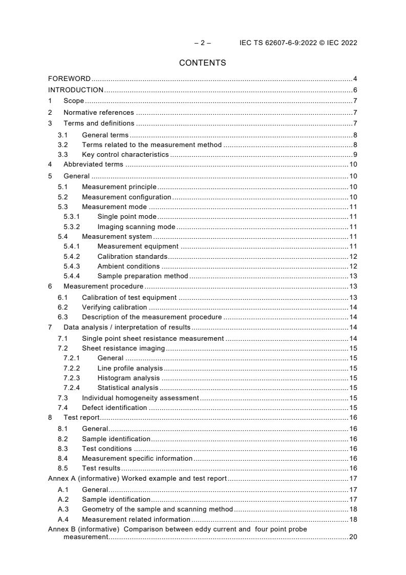
– 2 – IEC TS 62607-6-9:2022 © IEC 2022
CONTENTS
FOREWORD . 4
INTRODUCTION . 6
1 Scope . 7
2 Normative references . 7
3 Terms and definitions . 7
3.1 General terms . 8
3.2 Terms related to the measurement method . 8
3.3 Key control characteristics . 9
4 Abbreviated terms . 10
5 General . 10
5.1 Measurement principle . 10
5.2 Measurement configuration . 10
5.3 Measurement mode . 11
5.3.1 Single point mode . 11
5.3.2 Imaging scanning mode . 11
5.4 Measurement system . 11
5.4.1 Measurement equipment . 11
5.4.2 Calibration standards . 12
5.4.3 Ambient conditions . 12
5.4.4 Sample preparation method . 13
6 Measurement procedure . 13
6.1 Calibration of test equipment . 13
6.2 Verifying calibration . 14
6.3 Description of the measurement procedure . 14
7 Data analysis / interpretation of results . 14
7.1 Single point sheet resistance measurement . 14
7.2 Sheet resistance imaging . 15
7.2.1 General . 15
7.2.2 Line profile analysis . 15
7.2.3 Histogram analysis . 15
7.2.4 Statistical analysis . 15
7.3 Individual homogeneity assessment . 15
7.4 Defect identification . 15
8 Test report . 16
8.1 General . 16
8.2 Sample identification . 16
8.3 Test conditions . 16
8.4 Measurement specific information . 16
8.5 Test results . 16
Annex A (informative) Worked example and test report . 17
A.1 General . 17
A.2 Sample identification . 17
A.3 Geometry of the sample and scanning method . 18
A.4 Measurement related information . 18
Annex B (informative) Comparison between eddy current and four point probe
measurement . 20
B.1 General . 20
B.2 Results . 20
Annex C (informative) Use case quality inspection . 22
C.1 General . 22
C.2 Analysis of the sheet resistance distribution for quality inspection . 22
C.3 Analysis example . 22
Annex D (informative) Reference sample sets . 25
Bibliography . 26
Figure 1 – Scheme of measurement setup . 12
Figure A.1 – Sheet resistance map with histogram . 19
Figure B.1 – Correlation of the results of sheet resistance measured by the eddy
current (EC) method and by the four point probe (4PP) method . 21
Figure C.1 – Sheet resistance image of 200 mm × 200 mm graphene sheet . 22
Figure C.2 – Line profile analysis . 23
Figure C.3 – Histogram view of the whole sample . 23
Figure C.4 – Histogram analysis (high sheet resistance area) . 23
Figure C.5 – Histogram analysis (good area) . 24
Figure C.6 – Selective area analysis (used specified shape) . 24
Figure C.7 – Selective area analysis (regular shape) . 24
Figure D.1 – Sheet resistance reference sample set 300 mm × 300 mm . 25
Table A.1 – Product identification . 17
Table A.2 – General material description . 17
Table A.3 – Geometry of the sample and scanning parameter . 18
Table A.4 – Measurement related information . 18
Table A.5 – Test results: Sheet resistance . 18
Table B.1 – Comparison of the results of sheet resistance measured by the eddy
current method and by the four point probe method . 20
Table B.2 – Measurement accuracy . 21
– 4 – IEC TS 62607-6-9:2022 © IEC 2022
INTERNATIONAL ELECTROTECHNICAL COMMISSION
____________
NANOMANUFACTURING – KEY CONTROL CHARACTERISTICS –
Part 6-9: Graphene-based material – Sheet resistance:
Eddy current method
FOREWORD
1) The International Electrotechnical Commission (IEC) is a worldwide organization for standardization comprising
all national electrotechnical committees (IEC National Committees). The object of IEC is to promote international
co-operation on all questions concerning standardization in the electrical and electronic fields. To this end and
in addition to other activities, IEC publishes International Standards, Technical Specifications, Technical Reports,
Publicly Available Specifications (PAS) and Guides (hereafter referred to as "IEC Publication(s)"). Their
preparation is entrusted to technical committees; any IEC National Committee interested in the subject dealt with
may participate in this preparatory work. International, governmental and non-governmental organizations liaising
with the IEC also participate in this preparation. IEC collaborates closely with the International Organization for
Standardization (ISO) in accordance with conditions determined by agreement between the two organizations.
2) The formal decisions or agreements of IEC on technical matters express, as nearly as possible, an international
consensus of opinion on the relevant subjects since each technical committee has representation from all
interested IEC National Committees.
3) IEC Publications have the form of recommendations for international use and are accepted by IEC National
Committees in that sense. While all reasonable efforts are made to ensure that the technical content of IEC
Publications is accurate, IEC cannot be held responsible for the way in which they are used or for any
misinterpretation by any end user.
4) In order to promote international uniformity, IEC National Committees undertake to apply IEC Publications
transparently to the maximum extent possible in their national and regional publications. Any divergence between
any IEC Publication and the corresponding national or regional publication shall be clearly indicated in the latter.
5) IEC itself does not provide any attestation of conformity. Independent certification bodies provide conformity
assessment services and, in some areas, access to IEC marks of conformity. IEC is not responsible for any
services carried out by independent certification bodies.
6) All users should ensure that they have the latest edition of this publication.
7) No liability shall attach to IEC or its directors, employees, servants or agents including individual experts and
members of its technical committees and IEC National Committees for any personal injury, property damage or
other damage of any nature whatsoever, whether direct or indirect, or for costs (including legal fees) and
expenses arising out of the publication, use of, or reliance upon, this IEC Publication or any other IEC
Publications.
8) Attention is drawn to the Normative references cited in this publication. Use of the referenced publications is
indispensable for the correct application of this publication.
9) Attention is drawn to the possibility that some of the elements of this IEC Publication may be the subject of patent
rights. IEC shall not be held responsible for identifying any or all such patent rights.
IEC TS 62607-6-9 has been prepared by IEC technical committee 113: Nanotechnology for
electrotechnical products and systems. It is a Technical Specification.
The text of this Technical Specification is based on the following documents:
Draft Report on voting
113/569/DTS 113/625/RVDTS
Full information on the voting for its approval can be found in the report on voting indicated in
the above table.
The language used for the development of this Technical Specification is English.
This document was drafted in accordance with ISO/IEC Directives, Part 2, and developed in
accordance with ISO/IEC Directives, Part 1 and ISO/IEC Directives, IEC Supplement, available
at www.iec.ch/members_experts/refdocs. The main document types developed by IEC are
described in greater detail at www.iec.ch/standardsdev/publications.
A list of all parts in the IEC TS 62607 series, published under the general title
Nanomanufacturing – Key control characteristics, can be found on the IEC website.
The committee has decided that the contents of this document will remain unchanged until the
stability date indicated on the IEC website under webstore.iec.ch in the data related to the
specific document. At this date, the document will be
• reconfirmed,
• withdrawn,
• replaced by a revised edition, or
• amended.
IMPORTANT – The "colour inside" logo on the cover page of this document indicates that it
contains colours which are considered to be useful for the correct understanding of its
contents. Users should therefore print this document using a colour printer.
– 6 – IEC TS 62607-6-9:2022 © IEC 2022
INTRODUCTION
The application of graphene and graphene-related materials as a conductive large-area
electrode material has become of rising interest during recent years. Especially in the
application of graphene as a replacement material for indium tin oxide (ITO), graphene
combines low sheet resistance and high optical transparency. In particular, the application of
optically transparent large-area graphene layers has become more important. Hence, the
electrical characterization of large-area graphene layers is essential.
However, contacting methods, such as four-probe measurements, can cause damage to the
graphene and deteriorate its quality.
Non-contact methods have advantages for measurement of the sheet resistance since damage
to the layers is avoided and it is possible to readily scan the film to examine homogeneity.
The sheet resistance can serve as a measure for the electrical characterization due to its direct
dependence on conductivity and graphene quality for electrical applications.
NANOMANUFACTURING – KEY CONTROL CHARACTERISTICS –
Part 6-9: Graphene-based material – Sheet resistance:
Eddy current method
1 Scope
This part of IEC 62607 establishes a standardized method to determine the key control
characteristic
• sheet resistance
for films of graphene-based materials by
• eddy current method.
With this method a coil-generated primary alternating electromagnetic field induces eddy
currents in the conducting layer to be measured. The superposition of the primary field with the
secondary field induced by the eddy currents is a function of the sheet resistance of the layer.
– The method is applicable for the contactless measurement of the sheet resistance of large
area graphene layers on non-conductive substrates. As the method avoids any physical
contact, it prevents any mechanical damage to the sensitive graphene layer. Therefore, the
method is suitable for electrical characterization and quality control in an industrial
fabrication environment.
– Due to the use of two detectors – one above the substrate and one below the substrate –
the method is insensitive regarding small deviations from perfect flatness of the substrate.
– The range of graphene layers to be characterized comprises any quality, size and
morphology of graphene crystallites. Hence, the applicability of this method spans from high
quality, defect-free graphene layers to layers of dried graphene ink.
– The size of the graphene layers to be characterized includes layers larger than
25 mm × 25 mm for single point testing and 50 mm × 50 mm for imaging testing.
– The method can be used for layers of graphene-based material with a sheet resistance in
the nominal range of 10 Ω/sq to 5 000 Ω/sq.
2 Normative references
There are no normative references in this document.
3 Terms and definitions
For the purposes of this document, the following terms and definitions apply.
ISO and IEC maintain terminological databases for use in standardization at the following
addresses:
• IEC Electropedia: available at http://www.electropedia.org/
• ISO Online browsing platform: available at http://www.iso.org/obp
– 8 – IEC TS 62607-6-9:2022 © IEC 2022
3.1 General terms
3.1.1
graphene-based material
GBM
graphene material
grouping of carbon-based 2D materials that include one or more of graphene, bilayer graphene,
few-layer graphene, graphene nanoplate, and functionalized variations thereof as well as
graphene oxide and reduced graphene oxide.
Note 1 to entry: "Graphene material" is a short name for graphene-based material.
3.1.2
key control characteristic
KCC
key performance indicator
material property or intermediate product characteristic which can affect safety or compliance
with regulations, fit, function, performance, quality, reliability or subsequent processing of the
final product
Note 1 to entry: The measurement of a key control characteristic is described in a standardized measurement
procedure with known accuracy and precision.
Note 2 to entry: It is possible to define more than one measurement method for a key control characteristic, if the
correlation of the results is well-defined and known.
3.2 Terms related to the measurement method
3.2.1
eddy current
induced currents circulating along closed paths within a substance
[SOURCE: IEC 60050-121:1998, 121-12-32]
3.2.2
four point probe method
four terminal sensing
method to measure electrical sheet resistance or conductivity of thin films that uses separate
pairs of current-carrying and voltage-sensing electrodes
Note 1 to entry: The method is fast, repositionable and local.
Note 2 to entry: There is a comparison of eddy current (3.2.1) and four point probe methods in Annex B.
[SOURCE: ISO 80004-13:2017, 5.3.1, modified – Note 2 to entry has been added.]
3.2.3
inline four point probe method
type of four point probe measurement where four point electrodes are aligned in a row
Note 1 to entry: In this method, four probes contact the test sample in a linear arrangement. A voltage drop is
measured between the two inner probes while a current source supplies current through the outer probes.
Note 2 to entry: The thickness of the layer needs to be small compared to its lateral dimensions so that the sample
is approximately two-dimensional.
Note 3 to entry: The distance between the probes shall be small compared to the lateral dimensions of the sample
so that edge effects on the electric field in the sample can be neglected.
Note 4 to entry: The resistance of the sample can be calculated by Ohm's law. Geometrical factors can be used for
corrections if the sample is too small in size or if the measurement is performed close to the edges of the sample.
3.2.4
van der Pauw method
type of four probe measurement for samples of arbitrary shape
Note 1 to entry: The thickness of the layer needs to be small compared to its lateral dimensions so that the sample
is approximately two-dimensional.
Note 2 to entry: The van der Pauw method requires four probes placed arbitrarily around the perimeter of the
sample, in contrast to the linear four point probe which is placed on the top of the sample.
Note 3 to entry: The van der Pauw method provides an average sheet resistivity of the sample.
Note 4 to entry: The van der Pauw method relies on the assumption that the sample is homogeneous and
continuous.
3.2.5
surface conductance measurement using resonant cavity
method to measure the local surface conductance
Note 1 to entry: The measurements are made in an air filled standard R100 rectangular waveguide configuration,
at one of the resonant frequency modes, typically at 7 GHz.
Note 2 to entry: Surface conductance measurement by resonant cavity involves monitoring the resonant frequency
shift and change in the quality factor before and after insertion of the specimen into the cavity in a quantitative
correlation with the specimen surface area.
Note 3 to entry: The thickness of the specimen does not need to be known, but it is assumed that the lateral
dimension is uniform over the specimen area. This measurement is suited for atomically thin materials. Only resonant
frequency and the area of the specimen are measured. No calibration standards are required. Details are shown in
IEC TS 62607-6-4:2016.
Note 4 to entry: Resonance cavity methods and sheet resistance measurement methods do not deliver the same
information and therefore do not compete with each other. Resonance cavity methods are mainly used to assess
local defects and local properties whereas the sheet resistance measurements describe the electrical performance
of a film.
Note 5 to entry: Surface conductance measurement by resonance cavity method is obtained on a very small area
only. This technology is applied for the assessment of the individual performance, e.g. of a graphene flake.
Note 6 to entry: The above discussed sheet resistance measurement methods are measuring the ability of a larger
area to transport currents through an area requiring the currents to run through various flakes or areas. Here, the
number of grain boundaries, their electrical interconnectivity and the individual flake’s electrical property matter.
Note 7 to entry: Graphene films can have a good surface conductivity but can be unable to transport currents
through an area which is relevant for all applications where graphene is used for its electrical properties.
3.3 Key control characteristics
3.3.1
surface conductance
σ
S
sheet conductance
characteristic physical property of two-dimensional materials describing the ability to conduct
electric current
Note 1 to entry: The SI unit of measure of σ is siemens (S). In the trade and industrial literature, however, siemens
S
per square (S/sq) is commonly used when referring to surface conductance. "S/sq" is dimensionally equal to "S", but
is exclusively used for surface conductance to avoid confusion with electric conductance (G), which shares the same
unit of measure: G = I/U = σ ·(w/l).
S
Note 2 to entry: The surface conductance (σ ) can be obtained by normalizing conductance G to the specimen width
S
(w) and length (l).
3.3.2
surface resistance
ρ
S
sheet resistance
reciprocal of surface conductance, σ
S
– 10 – IEC TS 62607-6-9:2022 © IEC 2022
Note 1 to entry: ρ is a characteristic property of two-dimensional materials. The SI unit of measure of ρ is ohm (Ω).
S S
In the trade and industrial literature, however, ohm per square (Ω/sq) is commonly used when referring to surface
resistance or sheet resistance.
4 Abbreviated terms
4PP four point probe, test method
EC eddy current, test method
ITO
NIST National Institute o
...


Questions, Comments and Discussion
Ask us and Technical Secretary will try to provide an answer. You can facilitate discussion about the standard in here.
Loading comments...