IEC 60191-6:1990/AMD1:1999
(Amendment)Amendment 1 - Mechanical standardization of semiconductor devices - Part 6: General rules for the preparation of outline drawings of surface mounted semiconductor device packages
Amendment 1 - Mechanical standardization of semiconductor devices - Part 6: General rules for the preparation of outline drawings of surface mounted semiconductor device packages
General Information
- Status
- Published
- Publication Date
- 21-Dec-1999
- Technical Committee
- SC 47D - Semiconductor devices packaging
- Drafting Committee
- WG 1 - TC 47/SC 47D/WG 1
- Current Stage
- DELPUB - Deleted Publication
- Start Date
- 29-Sep-2004
- Completion Date
- 14-Feb-2026
Relations
- Effective Date
- 05-Sep-2023
Overview
IEC 60191-6:1990/AMD1:1999 is Amendment 1 to the IEC mechanical standardization series for semiconductor devices. It updates Part 6, which defines general rules for preparing outline drawings of surface-mounted semiconductor device packages. This amendment specifically adds two TSOP (Thin Small Outline Package) family drawing templates - TSOP Type1 and TSOP Type2 - and their recommended dimensional values and notes (Annexes A.5, A.6, B.2 and B.3).
Key topics
- Outline drawing rules: formalizes how to present package outlines, datums and reference planes for surface-mounted device (SMD) packages.
- TSOP package definitions: new annexes include detailed figures and definitions for TSOP Type1 and TSOP Type2.
- Datum and planes: definition and application of datum A, seating plane, and base plane used in mechanical drawings.
- Terminal geometry: terminal cross-section, length of soldered part (Lp), terminal width (b, b1), and plating details (Pb/Sn, Pd) with recommended thickness and tolerances.
- Pitch and coplanarity: terminal pitch (iei) options, positional tolerances (including Maximum Material Condition, MMC), and allowable coplanarity for solderability.
- Index area and positional areas: rules for index mark placement and terminal position areas (l2 max, b3 max, etc.).
- Recommended dimensional tables: Annex B includes recommended nominal and limit values for mounting/interchangeability and gauging (examples: E × HD families, L1, ZD formulas, standard terminal counts).
Applications
This amendment is practical for professionals involved in the mechanical and PCB aspects of semiconductor packaging:
- Package designers creating TSOP outline drawings and mechanical specifications.
- PCB layout engineers ensuring pad patterns and clearances match standardized package outlines.
- Test socket and tray designers using recommended L1 / G1 dimensions for mechanical fixtures.
- Component manufacturers and assembly engineers for consistent terminal plating, coplanarity, and solderability requirements.
- Quality and standards teams ensuring interchangeability and compliance with IEC mechanical rules.
Related standards
- This document is part of the IEC 60191 series (mechanical standardization of semiconductor devices) and was prepared by IEC TC47 / SC47D. For full compliance work, consult the full Part 6 text and other IEC 60191 parts for related package families.
Keywords: IEC 60191-6, TSOP, surface-mounted packages, outline drawings, semiconductor device packages, terminal pitch, coplanarity, datum A, mechanical standardization.
Buy Documents
IEC 60191-6:1990/AMD1:1999 - Amendment 1 - Mechanical standardization of semiconductor devices - Part 6: General rules for the preparation of outline drawings of surface mounted semiconductor device packages Released:12/22/1999 Isbn:2831850495
Frequently Asked Questions
IEC 60191-6:1990/AMD1:1999 is a standard published by the International Electrotechnical Commission (IEC). Its full title is "Amendment 1 - Mechanical standardization of semiconductor devices - Part 6: General rules for the preparation of outline drawings of surface mounted semiconductor device packages". This standard covers: Amendment 1 - Mechanical standardization of semiconductor devices - Part 6: General rules for the preparation of outline drawings of surface mounted semiconductor device packages
Amendment 1 - Mechanical standardization of semiconductor devices - Part 6: General rules for the preparation of outline drawings of surface mounted semiconductor device packages
IEC 60191-6:1990/AMD1:1999 is classified under the following ICS (International Classification for Standards) categories: 31.080.01 - Semiconductor devices in general. The ICS classification helps identify the subject area and facilitates finding related standards.
IEC 60191-6:1990/AMD1:1999 has the following relationships with other standards: It is inter standard links to IEC 60191-6:2004. Understanding these relationships helps ensure you are using the most current and applicable version of the standard.
IEC 60191-6:1990/AMD1:1999 is available in PDF format for immediate download after purchase. The document can be added to your cart and obtained through the secure checkout process. Digital delivery ensures instant access to the complete standard document.
Standards Content (Sample)
INTERNATIONAL IEC
STANDARD
60191-6
AMENDMENT 1
1999-12
Amendment 1
Mechanical standardization
of semiconductor devices –
Part 6:
General rules for the preparation
of outline drawings of surface mounted
semiconductor device packages
Amendement 1
Normalisation mécanique des dispositifs
à semiconducteurs –
Partie 6:
Règles générales pour la préparation des dessins
d'encombrement des dispositifs à semiconducteurs
à montage en surface
IEC 1999 Copyright - all rights reserved
International Electrotechnical Commission 3, rue de Varembé Geneva, Switzerland
Telefax: +41 22 919 0300 e-mail: inmail@iec.ch IEC web site http://www.iec.ch
Commission Electrotechnique Internationale
PRICE CODE
R
International Electrotechnical Commission
For price, see current catalogue
– 2 – 60191-6 Amend. 1 IEC:1999(E)
FOREWORD
This amendment has been prepared by subcommittee 47D: Mechanical standardization of
semiconductor devices, of IEC technical committee 47: Semiconductor devices.
The text of this amendment is based on the following documents:
FDIS Report on voting
47D/320/FDIS 47D/327/RVD
Full information on the voting for the approval of this amendment can be found in the report
on voting indicated in the above table.
A bilingual version of this amendment may be issued at a later date.
___________
Page 15
After subclause 4.4, add the following subclauses 4.5 and 4.6:
4.5 TSOP Type1
See annex A.5.
4.6 TSOP Type2
See annex A.6.
After subclause 5.1, add the following subclauses 5.2 and 5.3
5.2 TSOP Type1
See annex B.2.
5.3 TSOP Type2
See annex B.3.
60191-6 Amend. 1 IEC:1999(E) – 3 –
Page 31
Add, after Appendix A4, the following annexes A.5 and A.6.
– 4 – 60191-6 Amend. 1 IEC:1999(E)
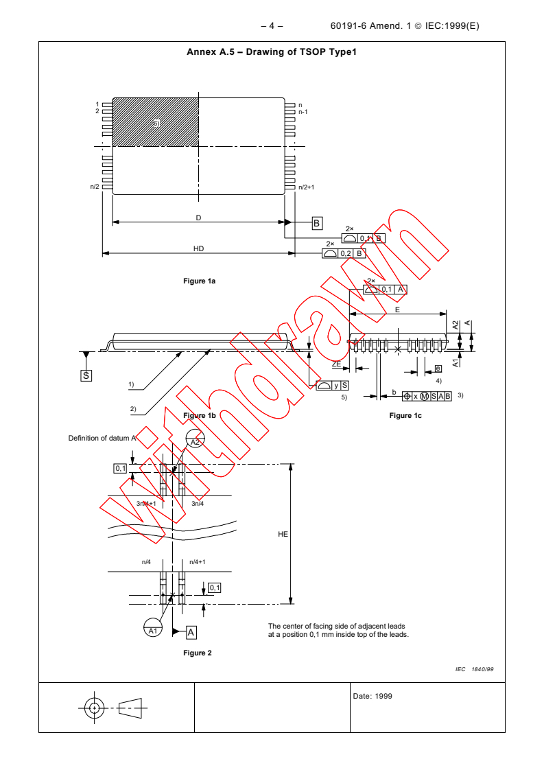
Annex A.5 – Drawing of TSOP Type1
n
n-1
6)
n/2 n/2+1
D
B
2×
0,1 B
2×
HD
0,2 B
2×
Figure 1a
0,1 A
E
ZE
e
S
4)
1)
y S
b
3)
x M S A B
5)
2)
Figure 1b Figure 1c
Definition of datum A
A2
0,1
3n/4
3n/4+1
HE
n/4 n/4+1
0,1
The center of facing side of adjacent leads
A1
A
at a position 0,1 mm inside top of the leads.
Figure 2
IEC 1840/99
Date: 1999
A1 A2
A
60191-6 Amend. 1 IEC:1999(E) – 5 –
Annex A.5 – Drawing of TSOP Type1
G1D
b
b1
(L)
7)
Terminal cross section
Lp
(L1)
Figure 3
IEC 1841/99
NOTES
1)
Seating plane.
2)
Base plane.
3)
The maximum material conditions apply to the positional tolerance of the terminals.
4)
Specifies the true geometric position of the terminal axis.
5)
Coplanarity. Specifies the allowable vertical distance of the lowest part of each terminal from the seating plane.
6)
Index area. Shows the allowable position of the index mark, which shall be included in the shaded area entirely.
7)
The dimensions of the terminal cross section apply to the ranges of 0,1 mm and 0,25 mm from the end of a terminal.
Date: 1999
θ
c
A3
c1
c
– 6 – 60191-6 Amend. 1 IEC:1999(E)
Annex A.5 – Drawing of TSOP Type1
l2 max = Lp max + 0,1
b3 max = b max + x
l2
b3
e
eD
Terminal position area
Figure 4
IEC 1842/99
Date: 1999
60191-6 Amend. 1 IEC:1999(E) – 7 –
Annex A.6 – Drawing of TSOP Type2
2×
0,1 B
n n-1 n/2+1
6)
2×
12 n/2
B
0,2 B
Figure 1a
2×
0,2 A
ZD
S y S 5)
e
b
4)
3)
x M S A B
1)
Figure 1c
2)
Figure 1b
Definition of datum A
1) For even number of leads 2) For odd number of leads
on package side. on package side.
A2 A2
0,1 0,1
3n/4+1 3n/4 (3n+2)/4
HE HE
n/4 n/4+1
(n+2)/4
0,1 0,1
A1 A1
A A
Figure 2a Figure 2b
The center of facing side of adjacent leads The center leads at a position 0,1 mm
at a position 0,1 mm inside top of the leads. inside top of the leads.
IEC 1843/99
Date: 1999
E
HE
A1 A2
A
– 8 – 60191-6 Amend. 1 IEC:1999(E)
Annex A.6 – Drawing of TSOP Type2
G1E
b
b1
L
7)
Terminal cross section
Lp
L1
Figure 3a Figure 3b
IEC 1844/99
NOTES
1)
Seating plane.
2)
Base plane.
3)
The maximum material conditions apply to the positional tolerance of the terminals.
4)
Specifies the true geometric position of the terminal axis.
5)
Coplanarity. Specifies the allowable vertical distance of the lowest part of each terminal from the seating plane.
6)
Index area. Shows the allowable position of the index mark, which shall be included in the shaded area entirely.
7)
The dimensions of the terminal cross section apply to the ranges of 0,1 mm and 0,25 mm from the end of a terminal.
Date: 1999
θ
c
A3
c1
c
60191-6 Amend. 1 IEC:1999(E) – 9 –
Annex A.6 – Drawing of TSOP Type2
l2 max = Lp max + 0,10
b3 max = b max + x
e
b3
Terminal position area
Figure 4
IEC 1845/99
Date: 1999
l2
eE
– 10 – 60191-6 Amend. 1 IEC:1999(E)
Page 37
Add, after Appendix B1, the following annex B.2.
Annex B.2
Recommended values for TSOP Type1, original dimensions: mm.
These recommendations apply to the packages illustrated by annex A.5 and to similar
packages.
Packages of this family are classified into types based on dimension E x HD.
60191-6 Amend. 1 IEC:1999(E) – 11 –
Group 1 – Dimensions appropriate to mounting and interchangeability
Recommended
Description Symbol Standard Remarks
values
6 × 14 8 × 14 14 × 20
6 × 16 8 × 16
6 × 18 8 × 18
Nominal 6 × 20 8 × 20
E × HD
—
dimensions
10 × 14 12 × 14
10 × 16 12 × 16
18 × 18 12 × 18
10 × 20 12 × 20
E = 6 + 2k
1)
Dimension E does not
k = 0,1,2,3,4
include resin fines and
kE gate remainders
2)
It is recommended that
Package 06,00
E
—
upper and lower cavities
width
18,00
be equal
2 10,00
3)
Mold protrusion is less
3 12,00
than 0,20 mm
4 14,00
1)
Dimension D does not
include resin fines and
gate remainders
Package 2)
It is recommended that
D D = HD – 2L1 nom —
length
upper and lower cavities
be equal. If they are
different, the larger
dimension shall be
regarded
1)
Package Min Nom Max Bend of package is
A2 —
height included
0,95 1,00 1,05
HD = 14 + 2 h
h = 0,1,2,3
hHD
Overall
HD 0 14,00 —
width
1 16,00
2 18,00
3 20,00
1)
Seated Min Nom Max Bend of package is
A —
height included
1,20
– 12 – 60191-6 Amend. 1 IEC:1999(E)
Group 1 (continued)
Recommended
Description Symbol Standard Remarks
values
Stand-off Min Nom Max
A1 —
height
0,05 0,10 0,15
Standard
height of
A3 A3 = 0,25 —
soldered
points
Length of Min Nom Max
Lp —
soldered
0,45 0,60 0,75
part
b nom
1)
b1 denotes the material
iei Min Nom Max
width of a lead frame
Pb/Sn
iei
Pd
0,65 0,17 0,32 Solder
2)
plating
b denotes the width of
plating
b 0,50 0,17 0,27
a plated terminal
0,65 0,24 0,22
0,40 0,13 0,23
3)
b1 and b apply to the
0,50 0,22 0,20
0,30 0,09 0,175
ranges of 0,1 and 0,25
0,40 0,18 0,16
from the end of a
0,30 0,14 0,12
terminal
Terminal
4)
Values b apply to Pb/Sn
width
solder plated terminal
The standard thickness
Min Nom Max of the solder layer shall
iei
+0,010
be 0,010
0,65 0,17 0,22 0,27 0,005
−
b1 0,50 0,17 0,20 0,23 —
5)
As Pd plating is very
0,40 0,13 0,16 0,19
thin, terminal width is
defined by b1 = b
0,30 0,09 0,12 0,15
1) 1)
Pb/Sn Solder c1 denotes the material
plating width of a lead frame
iei Min Nom Max
2)
c nom = 0,170
c denotes the width of
0,65 0,09 0,20
0,145 a plated terminal
c 0,50 0,09 0,20
0,120
3)
c1 and c apply to the
0,40 0,09 0,20
2)
Pd plating r
...


Questions, Comments and Discussion
Ask us and Technical Secretary will try to provide an answer. You can facilitate discussion about the standard in here.
Loading comments...