IEC TS 62607-5-4:2022
(Main)Nanomanufacturing - Key control characteristics - Part 5-4: Energy band gap measurement of nanomaterials by electron energy loss spectroscopy (EELS)
Nanomanufacturing - Key control characteristics - Part 5-4: Energy band gap measurement of nanomaterials by electron energy loss spectroscopy (EELS)
IEC TS 62607-5-4:2022 specifies the measuring method of the band gap energy of a nanomaterial using electron energy loss data of transmission electron microscope.
The method specified in this document is applicable to semiconducting and insulating nanomaterials to estimate the band gap.
The measurement to get reliable data is performed under the consistent conditions of TEM observation and specimen thickness. The applicable measurement range of band gap energy is more than 2 eV.
General Information
- Status
- Published
- Publication Date
- 06-Dec-2022
- Technical Committee
- TC 113 - Nanotechnology for electrotechnical products and systems
- Drafting Committee
- WG 3 - TC 113/WG 3
- Current Stage
- PPUB - Publication issued
- Start Date
- 07-Dec-2022
- Completion Date
- 12-Jan-2023
Overview
IEC TS 62607-5-4:2022 outlines a standardized method for measuring the energy band gap of nanomaterials using electron energy loss spectroscopy (EELS) with a transmission electron microscope (TEM). This technical specification, developed by the International Electrotechnical Commission (IEC), addresses the need for reliable, localized measurement of the band gap-an essential characteristic in advanced nanomanufacturing, particularly for semiconducting and insulating nanomaterials. The standard ensures that measurements are performed under consistent TEM observation conditions and with defined specimen thickness, targeting band gap energies greater than 2 eV.
Key Topics
- Band Gap Energy Measurement: Provides a method for determining the energy difference between the highest occupied and lowest unoccupied electronic states in nanomaterials, critical for electronic and optoelectronic properties.
- Applicability: Focuses on semiconducting and insulating nanomaterials, supporting the estimation of their band gap at nanometer-scale precision.
- Instrumentation: Describes the use of TEM in conjunction with EELS, specifying equipment calibration, specimen requirements, and detector choices (magnetic sector prism preferred for combined imaging and energy measurement).
- Sample Preparation: Stresses the importance of thin (<100 nm) specimens for accurate results and recommends surface coating for insulating samples to prevent charging.
- Test Procedure: Details stepwise alignment, imaging, electron beam positioning, and spectrum acquisition to ensure reproducible and interpretable results.
- Data Analysis: Guides users through spectrum normalization, baseline determination, linear fitting for band gap extraction, and comprehensive reporting, following best practices for accuracy and transparency.
Applications
Adopting IEC TS 62607-5-4:2022 allows manufacturers, researchers, and quality laboratories to:
- Characterize Nanomaterials: Precisely measure and report key electronic properties of nano-scale films and devices, enabling quality control in production lines and research laboratories.
- Optimize Device Performance: Support the development of new nano-enabled electronics, optoelectronics, and photovoltaic applications by enabling in situ and localized band gap measurements.
- Standardize Data: Facilitate comparison and benchmarking of nanomaterial properties across the industry by ensuring data reliability and consistency.
- Support Flexible and Multi-layer Devices: As devices shrink and adopt multi-layer structures, this standard addresses the complexity by allowing targeted measurement in specific device regions or layers.
Related Standards
To complement IEC TS 62607-5-4:2022, relevant additional standards include:
- IEC TS 62607 series: Covers a variety of key control characteristics for nanomanufacturing, such as purity, structure, and other electronic properties.
- ISO/TS 10797: For characterization of carbon nanotubes using TEM.
- ISO 29301 and ISO 25498: Offer analytical electron microscopy methods and diffraction analysis guidance.
- ISO/TS 80004-6: Provides terminology and definitions for nano-object characterization, supporting standardized communication.
Practical Value
Implementing IEC TS 62607-5-4:2022 in industrial and research settings enables organizations to:
- Achieve reliable, reproducible band gap measurements at the nanoscale
- Ensure data integrity and compatibility with global industry standards
- Enhance innovation in nanomaterial-based device engineering
- Streamline communication and reporting processes for regulatory and quality purposes
By adopting this IEC technical specification, the nanotechnology sector benefits from a unified methodology for assessing one of the most critical material properties, accelerating progress in next-generation electronic, optical, and energy devices.
Buy Documents
IEC TS 62607-5-4:2022 - Nanomanufacturing - Key control characteristics - Part 5-4: Energy band gap measurement of nanomaterials by electron energy loss spectroscopy (EELS) Released:12/7/2022
Frequently Asked Questions
IEC TS 62607-5-4:2022 is a technical specification published by the International Electrotechnical Commission (IEC). Its full title is "Nanomanufacturing - Key control characteristics - Part 5-4: Energy band gap measurement of nanomaterials by electron energy loss spectroscopy (EELS)". This standard covers: IEC TS 62607-5-4:2022 specifies the measuring method of the band gap energy of a nanomaterial using electron energy loss data of transmission electron microscope. The method specified in this document is applicable to semiconducting and insulating nanomaterials to estimate the band gap. The measurement to get reliable data is performed under the consistent conditions of TEM observation and specimen thickness. The applicable measurement range of band gap energy is more than 2 eV.
IEC TS 62607-5-4:2022 specifies the measuring method of the band gap energy of a nanomaterial using electron energy loss data of transmission electron microscope. The method specified in this document is applicable to semiconducting and insulating nanomaterials to estimate the band gap. The measurement to get reliable data is performed under the consistent conditions of TEM observation and specimen thickness. The applicable measurement range of band gap energy is more than 2 eV.
IEC TS 62607-5-4:2022 is classified under the following ICS (International Classification for Standards) categories: 07.030 - Physics. Chemistry; 07.120 - Nanotechnologies. The ICS classification helps identify the subject area and facilitates finding related standards.
IEC TS 62607-5-4:2022 is available in PDF format for immediate download after purchase. The document can be added to your cart and obtained through the secure checkout process. Digital delivery ensures instant access to the complete standard document.
Standards Content (Sample)
IEC TS 62607-5-4 ®
Edition 1.0 2022-12
TECHNICAL
SPECIFICATION
colour
inside
Nanomanufacturing – Key control characteristics –
Part 5-4: Energy band gap measurement of nanomaterials by electron energy
loss spectroscopy (EELS)
All rights reserved. Unless otherwise specified, no part of this publication may be reproduced or utilized in any form
or by any means, electronic or mechanical, including photocopying and microfilm, without permission in writing from
either IEC or IEC's member National Committee in the country of the requester. If you have any questions about IEC
copyright or have an enquiry about obtaining additional rights to this publication, please contact the address below or
your local IEC member National Committee for further information.
IEC Secretariat Tel.: +41 22 919 02 11
3, rue de Varembé info@iec.ch
CH-1211 Geneva 20 www.iec.ch
Switzerland
About the IEC
The International Electrotechnical Commission (IEC) is the leading global organization that prepares and publishes
International Standards for all electrical, electronic and related technologies.
About IEC publications
The technical content of IEC publications is kept under constant review by the IEC. Please make sure that you have the
latest edition, a corrigendum or an amendment might have been published.
IEC publications search - webstore.iec.ch/advsearchform IEC Products & Services Portal - products.iec.ch
The advanced search enables to find IEC publications by a Discover our powerful search engine and read freely all the
variety of criteria (reference number, text, technical publications previews. With a subscription you will always
committee, …). It also gives information on projects, replaced have access to up to date content tailored to your needs.
and withdrawn publications.
Electropedia - www.electropedia.org
IEC Just Published - webstore.iec.ch/justpublished
The world's leading online dictionary on electrotechnology,
Stay up to date on all new IEC publications. Just Published
containing more than 22 300 terminological entries in English
details all new publications released. Available online and
and French, with equivalent terms in 19 additional languages.
once a month by email.
Also known as the International Electrotechnical Vocabulary
(IEV) online.
IEC Customer Service Centre - webstore.iec.ch/csc
If you wish to give us your feedback on this publication or
need further assistance, please contact the Customer Service
Centre: sales@iec.ch.
IEC TS 62607-5-4 ®
Edition 1.0 2022-12
TECHNICAL
SPECIFICATION
colour
inside
Nanomanufacturing – Key control characteristics –
Part 5-4: Energy band gap measurement of nanomaterials by electron energy
loss spectroscopy (EELS)
INTERNATIONAL
ELECTROTECHNICAL
COMMISSION
ICS 07.030; 07.120 ISBN 978-2-8322-6199-6
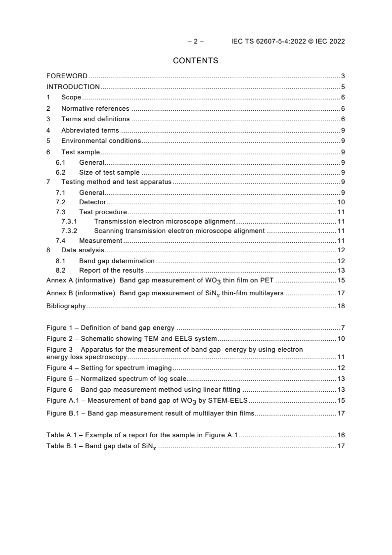
– 2 – IEC TS 62607-5-4:2022 © IEC 2022
CONTENTS
FOREWORD . 3
INTRODUCTION . 5
1 Scope . 6
2 Normative references . 6
3 Terms and definitions . 6
4 Abbreviated terms . 9
5 Environmental conditions . 9
6 Test sample . 9
6.1 General . 9
6.2 Size of test sample . 9
7 Testing method and test apparatus . 9
7.1 General . 9
7.2 Detector . 10
7.3 Test procedure . 11
7.3.1 Transmission electron microscope alignment . 11
7.3.2 Scanning transmission electron microscope alignment . 11
7.4 Measurement . 11
8 Data analysis . 12
8.1 Band gap determination . 12
8.2 Report of the results . 13
Annex A (informative) Band gap measurement of WO thin film on PET . 15
Annex B (informative) Band gap measurement of SiN thin-film multilayers . 17
x
Bibliography . 18
Figure 1 – Definition of band gap energy . 7
Figure 2 – Schematic showing TEM and EELS system . 10
Figure 3 – Apparatus for the measurement of band gap energy by using electron
energy loss spectroscopy . 11
Figure 4 – Setting for spectrum imaging . 12
Figure 5 – Normalized spectrum of log scale . 13
Figure 6 – Band gap measurement method using linear fitting . 13
Figure A.1 – Measurement of band gap of WO by STEM-EELS . 15
Figure B.1 – Band gap measurement result of multilayer thin films. 17
Table A.1 – Example of a report for the sample in Figure A.1 . 16
Table B.1 – Band gap data of SiN . 17
x
INTERNATIONAL ELECTROTECHNICAL COMMISSION
____________
NANOMANUFACTURING – KEY CONTROL CHARACTERISTICS –
Part 5-4: Energy band gap measurement of nanomaterials
by electron energy loss spectroscopy (EELS)
FOREWORD
1) The International Electrotechnical Commission (IEC) is a worldwide organization for standardization comprising
all national electrotechnical committees (IEC National Committees). The object of IEC is to promote international
co-operation on all questions concerning standardization in the electrical and electronic fields. To this end and
in addition to other activities, IEC publishes International Standards, Technical Specifications, Technical Reports,
Publicly Available Specifications (PAS) and Guides (hereafter referred to as “IEC Publication(s)”). Their
preparation is entrusted to technical committees; any IEC National Committee interested in the subject dealt with
may participate in this preparatory work. International, governmental and non-governmental organizations liaising
with the IEC also participate in this preparation. IEC collaborates closely with the International Organization for
Standardization (ISO) in accordance with conditions determined by agreement between the two organizations.
2) The formal decisions or agreements of IEC on technical matters express, as nearly as possible, an international
consensus of opinion on the relevant subjects since each technical committee has representation from all
interested IEC National Committees.
3) IEC Publications have the form of recommendations for international use and are accepted by IEC National
Committees in that sense. While all reasonable efforts are made to ensure that the technical content of IEC
Publications is accurate, IEC cannot be held responsible for the way in which they are used or for any
misinterpretation by any end user.
4) In order to promote international uniformity, IEC National Committees undertake to apply IEC Publications
transparently to the maximum extent possible in their national and regional publications. Any divergence between
any IEC Publication and the corresponding national or regional publication shall be clearly indicated in the latter.
5) IEC itself does not provide any attestation of conformity. Independent certification bodies provide conformity
assessment services and, in some areas, access to IEC marks of conformity. IEC is not responsible for any
services carried out by independent certification bodies.
6) All users should ensure that they have the latest edition of this publication.
7) No liability shall attach to IEC or its directors, employees, servants or agents including individual experts and
members of its technical committees and IEC National Committees for any personal injury, property damage or
other damage of any nature whatsoever, whether direct or indirect, or for costs (including legal fees) and
expenses arising out of the publication, use of, or reliance upon, this IEC Publication or any other IEC
Publications.
8) Attention is drawn to the Normative references cited in this publication. Use of the referenced publications is
indispensable for the correct application of this publication.
9) Attention is drawn to the possibility that some of the elements of this IEC Publication may be the subject of patent
rights. IEC shall not be held responsible for identifying any or all such patent rights.
IEC TS 62607-5-4 has been prepared by IEC technical committee 113: Nanotechnology for
electrotechnical products and systems. It is a Technical Specification.
The text of this Technical Specification is based on the following documents:
Draft Report on voting
113/513/DTS 113/594/RVDTS
Full information on the voting for its approval can be found in the report on voting indicated in
the above table.
The language used for the development of this Technical Specification is English.
– 4 – IEC TS 62607-5-4:2022 © IEC 2022
This document was drafted in accordance with ISO/IEC Directives, Part 2, and developed in
accordance with ISO/IEC Directives, Part 1 and ISO/IEC Directives, IEC Supplement, available
at www.iec.ch/members_experts/refdocs. The main document types developed by IEC are
described in greater detail at www.iec.ch/publications.
A list of all parts in the IEC TS 62607 series, published under the general title
Nanomanufacturing – Key control characteristics, can be found on the IEC website.
The committee has decided that the contents of this document will remain unchanged until the
stability date indicated on the IEC website under webstore.iec.ch in the data related to the
specific document. At this date, the document will be
• reconfirmed,
• withdrawn,
• replaced by a revised edition, or
• amended.
IMPORTANT – The 'colour inside' logo on the cover page of this publication indicates
that it contains colours which are considered to be useful for the correct understanding
of its contents. Users should therefore print this document using a colour printer.
INTRODUCTION
Electronic and electrical devices developed up to now have been fabricated by stacking a series
of active and/or passive layers on a specific substrate. The current trend in developing such
devices is the miniaturization of product size, whereas the basic structure of multilayers on a
substrate has not changed. Accordingly geometrical scales in the inner structure of a device
have been decreasing and some of the scales such as thickness of the layers have finally
reached a few nanometres. One of the key control characteristics (KCCs) is the band gap of an
active layer which enables the electron or hole transportation, excitation and emission of
electrons, etc. to be controlled.
The band gap is referred to as an energy gap, which means a difference between an energy
level in which electrons exist and an energy level in which electrons do not exist. Even though
the band gap of a material is intrinsic, the band gap of a nanomaterial is an extrinsic property
which represents its size-dependency. Therefore, the band gap of nanoscale materials needs
to be measured locally, in situ or in vitro.
For the band gap measurement application to nanomaterials, a specific region of a nanometre-
scale device or a single layer of the multi-layered structure, a transmission electron microscope
(TEM), which has atomic-scale image resolution, and electron energy loss spectroscopy (EELS),
which can measure energy loss of electrons, have in general been used.
In this document, a method of measuring the band gap energy at a specific location for a
nanomaterial by using TEM and EELS is proposed.
– 6 – IEC TS 62607-5-4:2022 © IEC 2022
NANOMANUFACTURING – KEY CONTROL CHARACTERISTICS –
Part 5-4: Energy band gap measurement of nanomaterials
by electron energy loss spectroscopy (EELS)
1 Scope
This part of IEC TS 62607 specifies the measuring method of the band gap energy of a
nanomaterial using electron energy loss data of transmission electron microscope.
The method specified in this document is applicable to semiconducting and insulating
nanomaterials to estimate the band gap.
The measurement to get reliable data is performed under the consistent conditions of TEM
observation and specimen thickness. The applicable measurement range of band gap energy
is more than 2 eV.
2 Normative references
There are no normative references in this document.
3 Terms and definitions
For the purposes of this document, the following terms and definitions apply.
ISO and IEC maintain terminological databases for use in standardization at the
...


Questions, Comments and Discussion
Ask us and Technical Secretary will try to provide an answer. You can facilitate discussion about the standard in here.
Loading comments...