IEC/IEEE 62659:2015
(Main)Nanomanufacturing - Large scale manufacturing for nanoelectronics
Nanomanufacturing - Large scale manufacturing for nanoelectronics
IEC/IEEE 62659:2015(E) provides a framework for introducing nanoelectronics into large scale, high volume production in semiconductor manufacturing facilities through the incorporation of nanomaterials (e.g. carbon nanotubes, graphene, quantum dots, etc.). Since semiconductor manufacturing facilities need to incorporate practices that maintain high yields, there are very strict requirements for how manufacturing is performed. Nanomaterials represent a potential contaminant in semiconductor manufacturing facilities and need to be introduced in a structured and methodical way.
General Information
- Status
- Published
- Publication Date
- 29-Sep-2015
- Technical Committee
- TC 113 - Nanotechnology for electrotechnical products and systems
- Drafting Committee
- WG 3 - TC 113/WG 3
- Current Stage
- PPUB - Publication issued
- Start Date
- 30-Sep-2015
- Completion Date
- 31-Oct-2015
Overview
IEC/IEEE 62659:2015 - Nanomanufacturing: Large scale manufacturing for nanoelectronics provides a practical framework for safely and reliably introducing nanomaterials (for example, carbon nanotubes, graphene, quantum dots) into high-volume semiconductor manufacturing. The standard addresses the structured, methodical steps required to incorporate nanoscale materials and processes while protecting the strict contamination and yield requirements of modern fabs.
Key topics and requirements
- Scope and purpose: Framework to integrate nanoelectronics into existing large-scale fabrication environments with minimal yield risk.
- Supply‑chain stages covered: Raw materials acquisition, materials processing, device design, IC fabrication, test/qualification, and end‑use.
- Nanomaterial characterization: Guidance on describing materials by composition, density, purity, size/dimensions, electrical properties, delivery medium, surface functionalization, particle size distribution, surface area, shape, and aggregation.
- Manufacturing process types: Distinguishes bottom‑up, top‑down, and hybrid nanomanufacturing approaches and their relationship across length scales.
- Contamination and yield control: Emphasizes that nanomaterials can act as contaminants in fabs; introduces practices and sequencing to manage introduction without compromising yields.
- Safety and environmental considerations: Identifies the need to address potential health, safety and environmental risks when scaling nanomaterials in production.
- Definitions and terminology: Aligns with nanoscale/ nanotechnology terms (e.g., nanoscale, nano‑object, nanostructure) to ensure consistent communication across suppliers and fabs.
Applications and who uses this standard
IEC/IEEE 62659 is intended for stakeholders involved in scaling nanoelectronics from lab to fab-level production:
- Semiconductor foundries and fabrication process engineers - to plan and qualify nanomaterials in high-volume lines while protecting yield.
- Device and IC designers - to understand manufacturability constraints when specifying nanoscale materials or structures.
- Nanomaterial suppliers and OEMs - to provide consistent characterization and delivery media required by fabs.
- Quality, safety and environmental managers - to assess contamination control, workplace safety and lifecycle impacts.
- Standards bodies and regulatory reviewers - as a basis for interoperable technical practice in nanoelectronics manufacturing.
Related standards
- ISO/TS 80004 series (nanotechnology vocabulary and terminology) is referenced for terms and definitions; consult other IEC/IEEE nanotechnology standards for complementary guidance on measurement, testing and safety.
Keywords: IEC/IEEE 62659, nanomanufacturing, nanoelectronics, semiconductor manufacturing, nanomaterials, contamination control, high‑volume production, carbon nanotubes, graphene, quantum dots, materials characterization.
Get Certified
Connect with accredited certification bodies for this standard

National Aerospace and Defense Contractors Accreditation Program (NADCAP)
Global cooperative program for special process quality in aerospace.

CARES (UK Certification Authority for Reinforcing Steels)
UK certification for reinforcing steels and construction.

DVS-ZERT GmbH
German welding certification society.
Sponsored listings
Frequently Asked Questions
IEC/IEEE 62659:2015 is a standard published by the International Electrotechnical Commission (IEC). Its full title is "Nanomanufacturing - Large scale manufacturing for nanoelectronics". This standard covers: IEC/IEEE 62659:2015(E) provides a framework for introducing nanoelectronics into large scale, high volume production in semiconductor manufacturing facilities through the incorporation of nanomaterials (e.g. carbon nanotubes, graphene, quantum dots, etc.). Since semiconductor manufacturing facilities need to incorporate practices that maintain high yields, there are very strict requirements for how manufacturing is performed. Nanomaterials represent a potential contaminant in semiconductor manufacturing facilities and need to be introduced in a structured and methodical way.
IEC/IEEE 62659:2015(E) provides a framework for introducing nanoelectronics into large scale, high volume production in semiconductor manufacturing facilities through the incorporation of nanomaterials (e.g. carbon nanotubes, graphene, quantum dots, etc.). Since semiconductor manufacturing facilities need to incorporate practices that maintain high yields, there are very strict requirements for how manufacturing is performed. Nanomaterials represent a potential contaminant in semiconductor manufacturing facilities and need to be introduced in a structured and methodical way.
IEC/IEEE 62659:2015 is classified under the following ICS (International Classification for Standards) categories: 07.030 - Physics. Chemistry; 07.120 - Nanotechnologies; 25.020 - Manufacturing forming processes. The ICS classification helps identify the subject area and facilitates finding related standards.
IEC/IEEE 62659:2015 is available in PDF format for immediate download after purchase. The document can be added to your cart and obtained through the secure checkout process. Digital delivery ensures instant access to the complete standard document.
Standards Content (Sample)
IEC/IEEE 62659 ®
Edition 1.0 2015-09
INTERNATIONAL
STANDARD
Nanomanufacturing – Large scale manufacturing for nanoelectronics
All rights reserved. Unless otherwise specified, no part of this publication may be reproduced or utilized in any form
or by any means, electronic or mechanical, including photocopying and microfilm, without permission in writing being
secured. Requests for permission to reproduce should be addressed to either IEC at the address below or IEC’s
member National Committee in the country of the requester or from IEEE.
IEC Central Office Institute of Electrical and Electronics Engineers, Inc.
3, rue de Varembé 3 Park Avenue
CH-1211 Geneva 20 New York, NY 10016-5997
Switzerland United States of America
Tel.: +41 22 919 02 11 stds.ipr@ieee.org
Fax: +41 22 919 03 00 www.ieee.org
info@iec.ch
www.iec.ch
About the IEC
The International Electrotechnical Commission (IEC) is the leading global organization that prepares and publishes
International Standards for all electrical, electronic and related technologies.
About the IEEE
IEEE is the world’s largest professional association dedicated to advancing technological innovation and excellence for
the benefit of humanity. IEEE and its members inspire a global community through its highly cited publications,
conferences, technology standards, and professional and educational activities.
About IEC/IEEE publications
The technical content of IEC/IEEE publications is kept under constant review by the IEC and IEEE. Please make sure
that you have the latest edition, a corrigendum or an amendment might have been published.
IEC Catalogue - webstore.iec.ch/catalogue Electropedia - www.electropedia.org
The stand-alone application for consulting the entire The world's leading online dictionary of electronic and
bibliographical information on IEC International Standards, electrical terms containing more than 30 000 terms and
Technical Specifications, Technical Reports and other definitions in English and French, with equivalent terms in
documents. Available for PC, Mac OS, Android Tablets 15 additional languages. Also known as the International
and iPad. Electrotechnical Vocabulary (IEV) online.
IEC publications search - www.iec.ch/searchpub IEC Glossary - std.iec.ch/glossary
The advanced search enables to find IEC publications by a More than 60 000 electrotechnical terminology entries in
variety of criteria (reference number, text, technical English and French extracted from the Terms and
committee,…). It also gives information on projects, Definitions clause of IEC publications issued since 2002.
replaced and withdrawn publications. Some entries have been collected from earlier publications
of IEC TC 37, 77, 86 and CISPR.
IEC Just Published - webstore.iec.ch/justpublished
Stay up to date on all new IEC publications. Just Published IEC Customer Service Centre - webstore.iec.ch/csc
details all new publications released. Available online and If you wish to give us your feedback on this publication or
also once a month by email. need further assistance, please contact the Customer
Service Centre: csc@iec.ch.
IEC/IEEE 62659 ®
Edition 1.0 2015-09
INTERNATIONAL
STANDARD
Nanomanufacturing – Large scale manufacturing for nanoelectronics
INTERNATIONAL
ELECTROTECHNICAL
COMMISSION
ICS 07.030; 25.020 ISBN 978-2-8322-2915-6
– 2 – IEC/IEEE 62659:2015
IEC/IEEE 2015
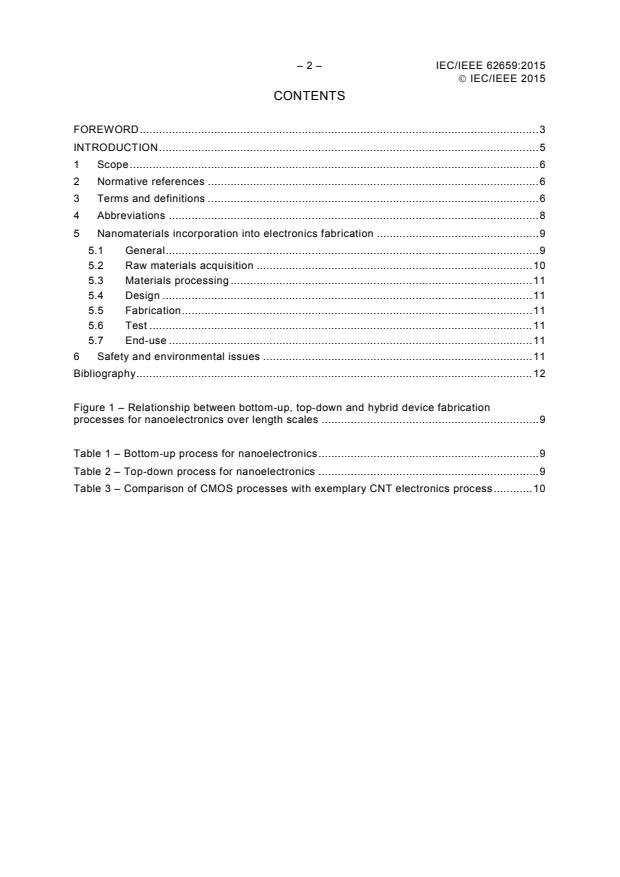
CONTENTS
FOREWORD . 3
INTRODUCTION . 5
1 Scope . 6
2 Normative references . 6
3 Terms and definitions . 6
4 Abbreviations . 8
5 Nanomaterials incorporation into electronics fabrication . 9
5.1 General . 9
5.2 Raw materials acquisition . 10
5.3 Materials processing . 11
5.4 Design . 11
5.5 Fabrication . 11
5.6 Test . 11
5.7 End-use . 11
6 Safety and environmental issues . 11
Bibliography . 12
Figure 1 – Relationship between bottom-up, top-down and hybrid device fabrication
processes for nanoelectronics over length scales . 9
Table 1 – Bottom-up process for nanoelectronics . 9
Table 2 – Top-down process for nanoelectronics . 9
Table 3 – Comparison of CMOS processes with exemplary CNT electronics process . 10
IEC/IEEE 2015
INTERNATIONAL ELECTROTECHNICAL COMMISSION
____________
NANOMANUFACTURING –
LARGE SCALE MANUFACTURING FOR NANOELECTRONICS
FOREWORD
1) The International Electrotechnical Commission (IEC) is a worldwide organization for standardization comprising
all national electrotechnical committees (IEC National Committees). The object of IEC is to promote
international co-operation on all questions concerning standardization in the electrical and electronic fields. To
this end and in addition to other activities, IEC publishes International Standards, Technical Specifications,
Technical Reports, Publicly Available Specifications (PAS) and Guides (hereafter referred to as “IEC
Publication(s)”). Their preparation is entrusted to technical committees; any IEC National Committee interested
in the subject dealt with may participate in this preparatory work. International, governmental and non-
governmental organizations liaising with the IEC also participate in this preparation.
IEEE Standards documents are developed within IEEE Societies and Standards Coordinating Committees of the
IEEE Standards Association (IEEE-SA) Standards Board. IEEE develops its standards through a consensus
development process, which brings together volunteers representing varied viewpoints and interests to achieve
the final product. Volunteers are not necessarily members of IEEE and serve without compensation. While IEEE
administers the process and establishes rules to promote fairness in the consensus development process, IEEE
does not independently evaluate, test, or verify the accuracy of any of the information contained in its
standards. Use of IEEE Standards documents is wholly voluntary. IEEE documents are made available for use
subject to important notices and legal disclaimers (see http://standards.ieee.org/IPR/disclaimers.html for more
information).
IEC collaborates closely with IEEE in accordance with conditions determined by agreement between the two
organizations.
2) The formal decisions of IEC on technical matters express, as nearly as possible, an international consensus of
opinion on the relevant subjects since each technical committee has representation from all interested IEC
National Committees. The formal decisions of IEEE on technical matters, once consensus within IEEE Societies
and Standards Coordinating Committees has been reached, is determined by a balanced ballot of materially
interested parties who indicate interest in reviewing the proposed standard. Final approval of the IEEE
standards document is given by the IEEE Standards Association (IEEE-SA) Standards Board.
3) IEC/IEEE Publications have the form of recommendations for international use and are accepted by IEC
National Committees/IEEE Societies in that sense. While all reasonable efforts are made to ensure that the
technical content of IEC/IEEE Publications is accurate, IEC or IEEE cannot be held responsible for the way in
which they are used or for any misinterpretation by any end user.
4) In order to promote international uniformity, IEC National Committees undertake to apply IEC Publications
(including IEC/IEEE Publications) transparently to the maximum extent possible in their national and regional
publications. Any divergence between any IEC/IEEE Publication and the corresponding national or regional
publication shall be clearly indicated in the latter.
5) IEC and IEEE do not provide any attestation of conformity. Independent certification bodies provide conformity
assessment services and, in some areas, access to IEC marks of conformity. IEC and IEEE are not responsible
for any services carried out by independent certification bodies.
6) All users should ensure that they have the latest edition of this publication.
7) No liability shall attach to IEC or IEEE or their directors, employees, servants or agents including individual
experts and members of technical committees and IEC National Committees, or volunteers of IEEE Societies
and the Standards Coordinating Committees of the IEEE Standards Association (IEEE-SA) Standards Board,
for any personal injury, property damage or other damage of any nature whatsoever, whether direct or indirect,
or for costs (including legal fees) and expenses arising out of the publication, use of, or reliance upon, this
IEC/IEEE Publication or any other IEC or IEEE Publications.
8) Attention is drawn to the normative references cited in this publication. Use of the referenced publications is
indispensable for the correct application of this publication.
9) Attention is drawn to the possibility that implementation of this IEC/IEEE Publication may require use of
material covered by patent rights. By publication of this standard, no position is taken with respect to the
existence or validity of any patent rights in connection therewith. IEC or IEEE shall not be held responsible for
identifying Essential Patent Claims for which a license may be required, for conducting inquiries into the legal
validity or scope of Patent Claims or determining whether any licensing terms or conditions provided in
connection with submission of a Letter of Assurance, if any, or in any licensing agreements are reasonable or
non-discriminatory. Users of this standard are expressly advised that determination of the validity of any patent
rights, and the risk of infringement of such rights, is entirely their own responsibility.
– 4 – IEC/IEEE 62659:2015
IEC/IEEE 2015
International Standard IEC/IEEE 62659 has been prepared by IEC technical committee 113,
Nanotechnology standardization for electrical and electronic products and systems, in
cooperation with the Standards Committee of the IEEE Nanotechnology Council , under the
IEC/IEEE Dual Logo Agreement.
The text of this standard is based on the following documents:
FDIS Report on voting
113/271/FDIS 113/280/RVD
Full information on the voting for the approval of this standard can be found in the report on
voting indicated in the above table.
International Standards are drafted in accordance with the rules given in the ISO/IEC
Directives, Part 2.
The IEC Technical Committee and IEEE Technical Committee have decided that the contents
of this publication will remain unchanged until the stability date indicated on the IEC web site
under "http://webstore.iec.ch" in the data related to the specific publication. At this date, the
publication will be
• reconfirmed,
• withdrawn,
• replaced by a revised edition, or
• amended.
A bilingual version of this publication may be issued at a later date.
—————————
A list of IEEE participants can be found at the following URL: http://standards.ieee.org/downloads/62659/62659-
2015/62659-2015_wg-participants.pdf
IEC/IEEE 2015
INTRODUCTION
In order to fully benefit from the cost, performance, and flexibility of new electronics products
manufactured on a large-scale, industries accustomed to the purchase, use, and engineering
of continuum materials need to grow to embrace appropriate new practices at the nanoscale.
The purpose of this International Standard is to enable the quick, low-risk adoption of
nanomaterials into large-scale electronics manufacturing. In addition a best set of common
practices for use by semiconductor fabricators will be delineated.
The description of nanomaterials to be incorporated into the electronics process can be
described in terms of: composition (material), density, purity, size/dimensions, properties
such as electrical characteristics (conductive, non-conductive, and semiconductive),
associated media (delivery medium), fabrication, surface functionalization, particle size
distribution, surface area, shape, and degree of aggregation and agglomeration, etc.
These standards for the characterization of nanomaterials also provide an opportunity to help
ensure consistency in metrics and measurement methods when specifying or producing
nanomaterials for electronics applications. This is important when multiple vendors or
technology partners are involved.
– 6 – IEC/IEEE 62659:2015
IEC/IEEE 2015
NANOMANUFACTURING –
LARGE SCALE MANUFACTURING FOR NANOELECTRONICS
1 Scope
This International Standard provides a framework for introducing nanoelectronics into large
scale, high volume production in semiconductor manufacturing facilities through the
incorporation of nanomaterials (e.g. carbon nanotubes, graphene, quantum dots, etc.). Since
semiconductor manufacturing facilities need to incorporate practices that maintain high yields,
there are very strict requirements for how manufacturing is performed. Nanomaterials
represent a potential contaminant in semiconductor manufacturing facilities and need to be
introduced in a structured and methodical way.
This International Standard provides steps employed to facilitate the introduction of
nanomaterials into the semiconductor manufacturing facilities. This sequence is described
below under the areas of raw materials acquisition, materials processing, design, IC
fabrication, testing, and end-use. These activities represent the major stages of the supply
chain in semiconductor manufacturing facilities.
2 Normative references
...


Questions, Comments and Discussion
Ask us and Technical Secretary will try to provide an answer. You can facilitate discussion about the standard in here.
Loading comments...