IEC 62899-203-2:2025
(Main)Printed electronics - Part 203-2: Materials - Semiconductor ink - Space charge limited mobility measurement in printed organic semiconductive layers
Printed electronics - Part 203-2: Materials - Semiconductor ink - Space charge limited mobility measurement in printed organic semiconductive layers
IEC 62899-203-2:2025 specifies a method to measure the values of effective charge carrier mobility in printed semiconductive layers using space charge limited current (SCLC) mobility technique. The method described is intended to be used as a benchmark test to allow reproducible measurements at a given temperature of the apparent charge carrier mobility for comparison with devices that use different materials, material formulations and fabrication processes for a planar configuration. This document specifies the sample and equipment requirements, and describes the measurement technique, the data analysis procedure and the reporting protocol.
This document is suitable to test unipolar devices (i.e. hole-only or electron-only), where charge injection is efficient and where series resistance does not dominate the current-voltage curve. Therefore, it cannot be used for testing high-electron mobility devices where electron injection can be problematic, for testing highly doped materials where space charge limited current does not exist, or to evaluate mobility in applications that require lateral charge transport, such as in transistors.
General Information
- Status
- Published
- Publication Date
- 18-Jun-2025
- Technical Committee
- TC 119 - Printed Electronics
- Drafting Committee
- WG 2 - TC 119/WG 2
- Current Stage
- PPUB - Publication issued
- Start Date
- 19-Jun-2025
- Completion Date
- 11-Jul-2025
Overview
IEC 62899-203-2:2025 - Printed electronics: Semiconductor ink - Space charge limited mobility measurement in printed organic semiconductive layers specifies a standardized test method to determine the effective charge carrier mobility of printed organic semiconductive layers using the space charge limited current (SCLC) technique. Designed as a reproducible benchmark at a specified temperature for planar devices, the standard defines sample and equipment requirements, the measurement procedure, data-analysis protocol and reporting format to enable consistent comparison between materials, formulations and fabrication processes.
Key topics and requirements
- Scope and limitations
- Intended for unipolar devices (hole-only or electron-only) with efficient charge injection and where series resistance does not dominate the I–V curve.
- Not suitable for devices with problematic electron injection, highly doped materials (no SCLC regime), or applications requiring lateral transport (e.g., transistors).
- Sample and DUT requirements
- Geometry and active area definitions for planar sandwich structures (thin semiconductive layer between parallel electrodes).
- Test equipment and measurement
- Protocol for stepwise voltage sweeps, current settling time, and temperature control to measure the I–V curve for SCLC analysis.
- Data analysis and corrections
- Procedures for series resistance checks, compensation for built‑in voltage, selection of valid data ranges, and least-squares fitting to extract the effective mobility.
- Recording of fit parameters, mobility values at specified electric fields, and fit images for traceability.
- Reporting
- A standardized reporting template and example (Annex A) to ensure reproducible, comparable results across labs.
Applications and users
- Materials R&D teams benchmarking semiconductor inks and printed organic semiconductive layers.
- Ink formulators and manufacturers evaluating formulation changes and process impacts on charge carrier mobility.
- Test laboratories and QA departments performing mobility measurements for product specification and supplier comparison.
- Academic and industrial researchers studying transport properties in printed electronics using the SCLC mobility technique.
Practical value
- Provides a reproducible, widely applicable benchmark for mobility in printed devices, improving comparability across vendors and publications.
- Reduces variability introduced by differing measurement practices and data-analysis methods, enabling better material selection for OLEDs, OPVs and other printed electronic components where vertical transport dominates.
Related standards
- IEC 62899-203 (Printed electronics - Part 203: Materials - Semiconductor ink)
- Other parts of the IEC 62899 series: IEC 62899-201 (Substrates), IEC 62899-202 (Conductive ink), IEC 62899-204 (Insulator ink)
Keywords: IEC 62899-203-2:2025, printed electronics, semiconductor ink, SCLC, space charge limited current, charge carrier mobility, mobility measurement, printed organic semiconductive layers.
Frequently Asked Questions
IEC 62899-203-2:2025 is a standard published by the International Electrotechnical Commission (IEC). Its full title is "Printed electronics - Part 203-2: Materials - Semiconductor ink - Space charge limited mobility measurement in printed organic semiconductive layers". This standard covers: IEC 62899-203-2:2025 specifies a method to measure the values of effective charge carrier mobility in printed semiconductive layers using space charge limited current (SCLC) mobility technique. The method described is intended to be used as a benchmark test to allow reproducible measurements at a given temperature of the apparent charge carrier mobility for comparison with devices that use different materials, material formulations and fabrication processes for a planar configuration. This document specifies the sample and equipment requirements, and describes the measurement technique, the data analysis procedure and the reporting protocol. This document is suitable to test unipolar devices (i.e. hole-only or electron-only), where charge injection is efficient and where series resistance does not dominate the current-voltage curve. Therefore, it cannot be used for testing high-electron mobility devices where electron injection can be problematic, for testing highly doped materials where space charge limited current does not exist, or to evaluate mobility in applications that require lateral charge transport, such as in transistors.
IEC 62899-203-2:2025 specifies a method to measure the values of effective charge carrier mobility in printed semiconductive layers using space charge limited current (SCLC) mobility technique. The method described is intended to be used as a benchmark test to allow reproducible measurements at a given temperature of the apparent charge carrier mobility for comparison with devices that use different materials, material formulations and fabrication processes for a planar configuration. This document specifies the sample and equipment requirements, and describes the measurement technique, the data analysis procedure and the reporting protocol. This document is suitable to test unipolar devices (i.e. hole-only or electron-only), where charge injection is efficient and where series resistance does not dominate the current-voltage curve. Therefore, it cannot be used for testing high-electron mobility devices where electron injection can be problematic, for testing highly doped materials where space charge limited current does not exist, or to evaluate mobility in applications that require lateral charge transport, such as in transistors.
IEC 62899-203-2:2025 is classified under the following ICS (International Classification for Standards) categories: 31.180 - Printed circuits and boards; 87.080 - Inks. Printing inks. The ICS classification helps identify the subject area and facilitates finding related standards.
IEC 62899-203-2:2025 is available in PDF format for immediate download after purchase. The document can be added to your cart and obtained through the secure checkout process. Digital delivery ensures instant access to the complete standard document.
Standards Content (Sample)
IEC 62899-203-2 ®
Edition 1.0 2025-06
INTERNATIONAL
STANDARD
Printed electronics -
Part 203-2: Materials - Semiconductor ink - Space charge limited mobility
measurement in printed organic semiconductive layers
ICS 31.180; 87.080 ISBN 978-2-8327-0493-6
All rights reserved. Unless otherwise specified, no part of this publication may be reproduced or utilized in any form or
by any means, electronic or mechanical, including photocopying and microfilm, without permission in writing from either
IEC or IEC's member National Committee in the country of the requester. If you have any questions about IEC copyright
or have an enquiry about obtaining additional rights to this publication, please contact the address below or your local
IEC member National Committee for further information.
IEC Secretariat Tel.: +41 22 919 02 11
3, rue de Varembé info@iec.ch
CH-1211 Geneva 20 www.iec.ch
Switzerland
About the IEC
The International Electrotechnical Commission (IEC) is the leading global organization that prepares and publishes
International Standards for all electrical, electronic and related technologies.
About IEC publications
The technical content of IEC publications is kept under constant review by the IEC. Please make sure that you have the
latest edition, a corrigendum or an amendment might have been published.
IEC publications search - IEC Products & Services Portal - products.iec.ch
webstore.iec.ch/advsearchform Discover our powerful search engine and read freely all the
The advanced search enables to find IEC publications by a
publications previews, graphical symbols and the glossary.
variety of criteria (reference number, text, technical With a subscription you will always have access to up to date
committee, …). It also gives information on projects, content tailored to your needs.
replaced and withdrawn publications.
Electropedia - www.electropedia.org
IEC Just Published - webstore.iec.ch/justpublished The world's leading online dictionary on electrotechnology,
Stay up to date on all new IEC publications. Just Published containing more than 22 500 terminological entries in English
details all new publications released. Available online and and French, with equivalent terms in 25 additional languages.
once a month by email. Also known as the International Electrotechnical Vocabulary
(IEV) online.
IEC Customer Service Centre - webstore.iec.ch/csc
If you wish to give us your feedback on this publication or
need further assistance, please contact the Customer
Service Centre: sales@iec.ch.
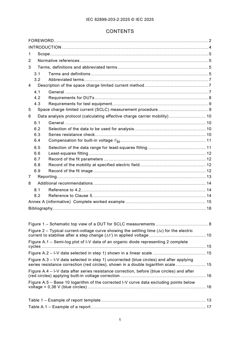
CONTENTS
FOREWORD . 2
INTRODUCTION . 4
1 Scope . 5
2 Normative references . 5
3 Terms, definitions and abbreviated terms . 5
3.1 Terms and definitions . 5
3.2 Abbreviated terms. 7
4 Description of the space charge limited current method . 7
4.1 General . 7
4.2 Requirements for DUTs . 8
4.3 Requirements for test equipment . 9
5 Space charge limited current (SCLC) measurement procedure . 9
6 Data analysis protocol (calculating effective charge carrier mobility) . 10
6.1 General . 10
6.2 Selection of the data to be used for analysis . 10
6.3 Series resistance check. 10
6.4 Compensation for built-in voltage V . 11
bi
6.5 Selection of the data range for least-squares fitting . 11
6.6 Least-squares fitting . 12
6.7 Record of the fit parameters . 12
6.8 Record of the mobility at specified electric field. 12
6.9 Record of the fit image . 12
7 Reporting . 13
8 Additional recommendations . 14
8.1 Reference to 4.2 . 14
8.2 Reference to Clause 5. 14
Annex A (informative) Complete worked example . 15
Bibliography . 18
Figure 1 – Schematic top view of a DUT for SCLC measurements . 8
Figure 2 – Typical current-voltage curve showing the settling time (∆t) for the electric
current to stabilise after a step change (∆V) in applied voltage . 10
Figure A.1 – Semi-log plot of I-V data of an organic diode representing 2 complete
cycles . 15
Figure A.2 – I-V data selected in step 1) shown in a linear scale . 15
Figure A.3 – I-V data selected in step 1) uncorrected (blue circles) and after applying
series resistance correction (red circles), shown in a double logarithm scale . 15
Figure A.4 – I-V data after series resistance correction, before (blue circles) and after
(red circles) applying built-in voltage correction . 16
Figure A.5 – Base 10 logarithm of the corrected I-V curve data excluding points below
voltage = 0,36 V (blue circles) . 16
Table 1 – Example of report template . 13
Table A.1 – Example of a report . 17
INTERNATIONAL ELECTROTECHNICAL COMMISSION
____________
Printed electronics -
Part 203-2: Materials - Semiconductor ink -
Space charge limited mobility measurement
in printed organic semiconductive layers
FOREWORD
1) The International Electrotechnical Commission (IEC) is a worldwide organization for standardization comprising
all national electrotechnical committees (IEC National Committees). The object of IEC is to promote international
co-operation on all questions concerning standardization in the electrical and electronic fields. To this end and
in addition to other activities, IEC publishes International Standards, Technical Specifications, Technical Reports,
Publicly Available Specifications (PAS) and Guides (hereafter referred to as "IEC Publication(s)"). Their
preparation is entrusted to technical committees; any IEC National Committee interested in the subject dealt with
may participate in this preparatory work. International, governmental and non-governmental organizations liaising
with the IEC also participate in this preparation. IEC collaborates closely with the International Organization for
Standardization (ISO) in accordance with conditions determined by agreement between the two organizations.
2) The formal decisions or agreements of IEC on technical matters express, as nearly as possible, an international
consensus of opinion on the relevant subjects since each technical committee has representation from all
interested IEC National Committees.
3) IEC Publications have the form of recommendations for international use and are accepted by IEC National
Committees in that sense. While all reasonable efforts are made to ensure that the technical content of IEC
Publications is accurate, IEC cannot be held responsible for the way in which they are used or for any
misinterpretation by any end user.
4) In order to promote international uniformity, IEC National Committees undertake to apply IEC Publications
transparently to the maximum extent possible in their national and regional publications. Any divergence between
any IEC Publication and the corresponding national or regional publication shall be clearly indicated in the latter.
5) IEC itself does not provide any attestation of conformity. Independent certification bodies provide conformity
assessment services and, in some areas, access to IEC marks of conformity. IEC is not responsible for any
services carried out by independent certification bodies.
6) All users should ensure that they have the latest edition of this publication.
7) No liability shall attach to IEC or its directors, employees, servants or agents including individual experts and
members of its technical committees and IEC National Committees for any personal injury, property damage or
other damage of any nature whatsoever, whether direct or indirect, or for costs (including legal fees) and
expenses arising out of the publication, use of, or reliance upon, this IEC Publication or any other IEC
Publications.
8) Attention is drawn to the Normative references cited in this publication. Use of the referenced publications is
indispensable for the correct application of this publication.
9) IEC draws attention to the possibility that the implementation of this document may involve the use of (a)
patent(s). IEC takes no position concerning the evidence, validity or applicability of any claimed patent rights in
respect thereof. As of the date of publication of this document, IEC had not received notice of (a) patent(s), which
may be required to implement this document. However, implementers are cautioned that this may not represent
the latest information, which may be obtained from the patent database available at https://patents.iec.ch. IEC
shall not be held responsible for identifying any or all such patent rights.
IEC 62899-203-2 has been prepared by IEC technical committee 119: Printed Electronics. It is
an International Standard.
The text of this International Standard is based on the following documents:
Draft Report on voting
119/541/FDIS 119/547/RVD
Full information on the voting for its approval can be found in the report on voting indicated in
the above table.
The language used for the development of this International Standard is English.
This document was drafted in accordance with ISO/IEC Directives, Part 2, and developed in
accordance with ISO/IEC Directives, Part 1 and ISO/IEC Directives, IEC Supplement, available
at www.iec.ch/members_experts/refdocs. The main document types developed by IEC are
described in greater detail at www.iec.ch/publications.
A list of all parts in the IEC 62899 series, published under the general title Printed electronics,
can be found on the IEC website.
The committee has decided that the contents of this document will remain unchanged until the
stability date indicated on the IEC website under webstore.iec.ch in the data related to the
specific document. At this date, the document will be
• reconfirmed,
• withdrawn, or
• revised.
INTRODUCTION
The IEC 62899-20x series relates mainly to evaluation methods for materials of printed
electronics. The series also includes storage methods, packaging and marking, and
transportation conditions.
The IEC 62899-20x series is divided into parts according to each material. Each part is prepared
as a generic specification containing fundamental information for the area of printed electronics.
The IEC 62899-20x series consists of the following parts:
IEC 62899-201, Printed electronics – Part 201: Materials – Substrates
IEC 62899-202, Printed electronics – Part 202: Materials – Conductive ink
IEC 62899-203, Printed electronics – Part 203: Materials – Semiconductor ink
IEC 62899-204, Printed electronics – Part 204: Materials – Insulator ink – Measurement
methods of properties of insulator inks and printed insulating layers
Furthermore, sectional specifications, blank detail specifications, and detail specifications of
each material will follow these parts.
(Subsequent parts will be prepared for other materials.)
Published literature has demonstrated a significant lack of reproducibility in the determination
of value of charge mobility in semiconductive materials when a standardised protocol for testing
and data analysis is not used, making benchmarking between semiconducting materials
challenging.[1]
This document focuses on the determination of charge mobility of semiconductive materials
used in printed electronics and contains a standardized protocol for the test conditions, the data
analysis method and the reporting procedure.
___________
Numbers in square brackets refer to the Bibliography.
1 Scope
This part of IEC 62899 specifies a method to measure the values of effective charge carrier
mobility in printed semiconductive layers using space charge limited current (SCLC) mobility
technique. The method described is intended to be used as a benchmark test to allow
reproducible measurements at a given temperature of the apparent charge carrier mobility for
comparison with devices that use different materials, material formulations and fabrication
processes for a planar configuration. This document specifies the sample and equipment
requirements, and describes the measurement technique, the data analysis procedure and the
reporting protocol.
This document is suitable to test unipolar devices (i.e. hole-only or electron-only), where charge
injection is efficient and where series resistance does not dominate the current-voltage curve.
Therefore, it cannot be used for testing high-electron mobility devices where electron injection
can be problematic, for testing highly doped materials where space charge limited current does
not exist, or to evaluate mobility in applications that require lateral charge transport, such as in
transistors.
2 Normative references
The following documents are referred to in the text in such a way that some or all of their content
constitutes requirements of this document. For dated references, only the edition cited applies.
For undated references, the latest edition of the referenced document (including any
amendments) applies.
IEC 62899-203, Printed electronics – Part 203: Materials – Semiconductor ink
3 Terms, definitions and abbreviated terms
3.1 Terms and definitions
For the purposes of this document, the terms and definitions given in IEC 62899-203 and the
following apply.
ISO and IEC maintain terminology databases for use in standardization at the following
addresses:
• IEC Electropedia: available at https://www.electropedia.org/
• ISO Online browsing platform: available at https://www.iso.org/obp
3.1.1
semiconductive material
ingredient of a printing or coating material, which itself is electrically semi-conductive
3.1.2
semiconductor ink
liquid in which one or more of particles, small molecules or polymers are dissolved or dispersed,
and which becomes an electrically semiconductive layer by solvent removal and/or post
treatment such as UV, photonic, or thermal processing
[SOURCE IEC 62899-101:2019 [2], 3.121]
3.1.3
semiconductive layer
film-like semiconductive body of material made of semiconductor ink (3.1.2), which is printed or
coated on a substrate, followed as necessary using a post treatment such as UV, photonic, or
thermal processing
[SOURCE IEC 62899-101:2019 [2], 3.119]
3.1.4
semiconductive film
substrate (sheet or roll) with semiconductive layer (3.1.3)
[SOURCE IEC 62899-101:2019 [2], 3.120]
3.1.5
(drift) mobility (of a charge carrier)
quantity equal to the quotient of the modulus of the mean velocity of a charge carrier in the
direction of an electric field by the modulus of the field strength
[SOURCE: IEC 60050:521:2002 [3], 521-02-58]
3.1.6
effective charge carrier mobility
equivalent single value of mobility that is representative of the device under test and reported
at a specified electric field to enable a single-valued comparison with other such devices
Note 1 to entry: The effective charge carrier mobility is a benchmark.
3.1.7
device under test
DUT
semiconducting device used to evaluate the charge mobility of the semiconducting material
Note 1 to entry: A thin semiconductive layer sandwiched between two parallel planar electrodes constitutes the
DUT structure.
3.1.8
electron-only device
semiconductor device in which the majority charge carriers are electrons, and minority carrier
injection is blocked such that the contribution to space charge from minority carriers and doping
is insignificant over the voltage range of interest
3.1.9
hole-only device
semiconductor device in which the majority charge carriers are holes, and the minority carrier
injection is blocked such that the contribution to space charge from the minority carriers and
doping is insignificant over the voltage range of interest
3.1.10
active device area
area defined by the overlap of parallel planar electrodes used to determine the current density
from the measured current
3.1.11
current-voltage curve
I-V curve
curve created from a sequence of measurements of device current at different applied external
voltages usually recorded in a stepwise voltage sweep operation
3.2 Abbreviated terms
DUT device under test
HOMO highest occupied molecular orbital
LUMO lowest unoccupied molecular orbital
OLED organic light emitting diode
OPVD organic photovoltaic device
SCLC space charge limited current
4 Description of the space charge limited current method
4.1 General
Charge (drift) mobility is a key parameter for performance assessment of semiconductive
materials that strongly depends on how the materials are processed. Therefore, it is important
to measure it in a device configuration that closely reproduces conditions relevant to the device
application.
The space charge limited current (SCLC) method is a steady-state technique which is well
suited for screening applications where the aim is to compare charge carrier mobility values
between different materials, material formulations and device fabrication processes. The
method is applied on a "sandwich" semiconductor device structure comprising a thin
semiconductive layer between two parallel planar electrodes (Figure 1). As such, the SCLC
method is suitable for evaluating semiconductive layers used in diode applications which
include organic photovoltaic devices (OPVDs) and organic light emitting diodes (OLEDs).
The SCLC mobility measurements are performed by measuring the steady-state current-voltage
(I-V) curves and fitting the data with Formula (1) by varying the μ and γ fitting parameters with
other parameters (i.e., V, d, ε) which are known or assumed. This formula was demonstrated to
provide reproducible results when the conditions required below are met, while, at the same
time, being simple to use [1]. Formula (1) assumes that the charge carrier mobility depends on
the electric field and that the electric field is not co
...


Questions, Comments and Discussion
Ask us and Technical Secretary will try to provide an answer. You can facilitate discussion about the standard in here.
Loading comments...