


Printed Circuits and Connectors: Essential Standards for Modern Electronics
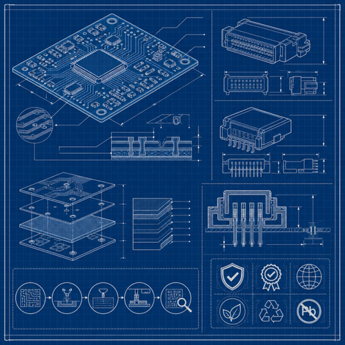
Electronics are at the heart of our digital economy—from mobile devices and computers to sophisticated industrial automation and smart vehicles. As the demand for smaller, more reliable, and more complex printed circuits and connectors grows, so does the necessity for robust, international standards. This article introduces you to four key IEC standards that define the terminology, material requirements, testing methods, and best practices that underpin modern printed circuit boards (PCBs), connectors, and assemblies. By embracing these standards, businesses not only boost quality and security but also set themselves up for productivity, scalability, and long-term success in today’s competitive landscape.
Overview / Introduction
Printed circuit boards and connectors form the essential backbone of electronic hardware, enabling the seamless interconnection of components for everything from smart watches to industrial robots. As miniaturization and complexity increase, so do the challenges for designers, manufacturers, and quality assurance professionals. International standards set by the IEC (International Electrotechnical Commission) provide a globally recognized foundation for achieving interoperability, safety, and reliability. In this guide, you’ll discover:
- Why each standard is essential to the electronics ecosystem
- What key requirements and specifications are outlined
- The practical benefits of standardization for businesses and end-users
- How these guidelines underpin quality control, production efficiency, and compliance
By the end, you’ll see how adopting these standards can unlock higher productivity, enhanced security, and scalable operations in your organization.
Detailed Standards Coverage
IEC 60194:1999 – The Language of Printed Circuit Boards
Printed board design, manufacture and assembly – Terms and definitions
Modern electronics are a tapestry of complex processes and components. For engineers, manufacturers, and suppliers to work together effectively, precise and consistent terminology is critical. That’s the role of IEC 60194:1999—it brings clarity to the language of PCBs and their assemblies.
Scope and Key Features: This standard defines the key vocabulary used for printed boards and their assemblies, covering over a thousand terms, classifications, and graphical symbols. It aligns with IEC’s International Electrotechnical Vocabulary (IEV), ensuring global consistency. The terms span:
- PCB types and structures
- Materials (substrates, laminates, coatings)
- Manufacturing processes (etching, bonding, plating)
- Assembly practices (mounting, soldering, testing)
- Quality and inspection terminology
Who Should Use It:
- PCB designers and layout engineers
- Quality assurance and production teams
- Procurement and supply chain professionals
- Electronic product developers across industries
Practical Implications: Adopting this standard ensures that all stakeholders—regardless of language or background—can communicate with precision, reducing errors and improving design transfer, manufacturing, and quality control processes.
Key highlights:
- Unifies technical language for global supply chain integration
- Enhances accuracy in documentation, designs, and contracts
- Reduces misinterpretation, saving costs and time in manufacturing
Access the full standard:View IEC 60194:1999 on iTeh Standards
IEC 61249-3-6:2026 – Material Specification for PTFE-Filled Laminates
Materials for circuit boards and other interconnecting structures – Part 3-6: Sectional specification set for unreinforced base materials clad and unclad – Polytetrafluoroethylene (PTFE) filled laminate sheets of defined flammability (vertical burning test), copper-clad
As the demand for high-speed, high-frequency circuits increases, materials like polytetrafluoroethylene (PTFE) play a central role. IEC 61249-3-6:2026 establishes the requirements for PTFE-filled, unreinforced laminates—critical substrates for RF and microwave PCBs.
What This Standard Covers:
- Specifies properties for sheets ranging from 0.02 mm to 3.2 mm thickness, both copper-clad and unclad
- Defines flammability performance using vertical burning tests (critical for safety and regulatory compliance)
- Covers requirements on electrical and non-electrical properties, such as surface and volume resistivity, dielectric constant, dissipation factors, mechanical stability, and more
- Sets out test methods for appearance (pits, dents, scratches), dimensional tolerances, bonding strength, heat shock, water absorption, and degradation temperature
Who Needs to Comply:
- PCB manufacturers supplying to the telecommunications, aerospace, automotive, and industrial sectors
- Designers working on RF, microwave, and high-reliability electronics
- Material suppliers and procurement teams assessing laminate suitability
Key Implementation Insights:
- Ensures consistent, high-performance substrate materials that meet demanding electrical and mechanical requirements
- Facilitates global sourcing and regulatory approval with harmonized flammability and material performance criteria
- Enables traceability and reliability for mission-critical applications
Key highlights:
- Comprehensive specifications for PTFE-laminate thickness, dielectric properties, and bonding
- Defined safety and flammability thresholds for global compliance
- Detailed testing, quality assurance, and reporting requirements
Access the full standard:View IEC 61249-3-6:2026 on iTeh Standards
IEC 62899-204:2019 – Measurement Methods for Insulator Inks in Printed Electronics
Printed electronics – Part 204: Materials – Insulator ink – Measurement methods of properties of insulator inks and printed insulating layers
Printed electronics represents the next frontier in flexible, low-cost device manufacturing. For these designs to thrive in consumer and industrial products, the properties of insulating inks and printed dielectric layers must be rigorously controlled.
What the Standard Offers:
- Defines terms and standard methods for characterizing and evaluating insulator inks and their printed layers
- Covers key measurements, including density, rheology (viscosity), surface tension, and flash point for inks
- Details test protocols for printed insulating layers, such as volume resistivity, dielectric constant, electric strength, and optical properties (like transparency and haze)
- Specifies storage conditions and how to measure deterioration over time
Who Benefits from this Standard:
- Manufacturers of printed and flexible electronics (wearables, smart packaging, sensors)
- Ink developers formulating new insulating or dielectric compounds
- Quality assurance labs and R&D teams evaluating material suitability
Practical Benefits:
- Ensures reproducibility and quality across batches and between global suppliers
- Minimizes performance variability due to material stability or process variation
- Supports third-party validation and industry certification
Key highlights:
- Standardized test methods for all major insulator ink and film properties
- Compatible with international best practices in printed/flexible electronics
- Guidance for optimal storage and longevity of materials
Access the full standard:View IEC 62899-204:2019 on iTeh Standards
IEC TR 61189-5-506:2019 – Testing Surface Insulation Resistance in Fine-Pitch Assemblies
Test methods for electrical materials, printed boards and other interconnection structures and assemblies – Part 5-506: General test methods for materials and assemblies – An intercomparison evaluation to implement the use of fine-pitch test structures for surface insulation resistance (SIR) testing of solder fluxes in accordance with IEC 61189-5-501
With the relentless drive to make electronics smaller and denser, fine-pitch structures are now standard in commercial and industrial products. Soldering residues and moisture can threaten surface insulation and lead to electrochemical migration and potential device failure. IEC TR 61189-5-506:2019 is a technical report that validates new, fine-pitch SIR test patterns.
Key Aspects:
- Details the development and benchmarking of a new 200-μm gap pattern for SIR testing (compared with standard 318 μm and 500 μm patterns)
- Describes protocols for preparing test boards, applying fluxes, and measuring resistance in high humidity/temperature environments to simulate real-world stresses
- Provides statistical data from international intercomparison studies across multiple labs
Who Needs This Standard:
- PCB and assembly manufacturers working with high-density and fine-pitch designs
- Quality assurance teams responsible for process validation
- Solder paste and flux suppliers seeking third-party validation of residue performance
Implementation Insights:
- Ensures that SIR tests accurately reflect the challenges posed by fine-pitch assemblies
- Provides a scientific basis for assessing electrochemical reliability of soldering materials and processes
- Supports the migration to advanced product geometries without sacrificing quality or compliance
Key highlights:
- Validates the use of fine-pitch (200 μm) SIR patterns for next-generation electronics
- Enables direct comparison with legacy test patterns for quality assurance
- Extensive international round-robin ensures reliability of results
Access the full standard:View IEC TR 61189-5-506:2019 on iTeh Standards
Industry Impact & Compliance
How Standards Transform Electronics Business Operations
Quality Control: Each of these standards underpins robust, repeatable quality controls—critical for reducing defects, managing supply chain complexity, and meeting regulatory requirements worldwide.
Global Market Access: Harmonized standards open doors to international markets, simplify procurement, reduce incompatibility risks and are often required for selling into regulated industries such as automotive, aerospace, and medical devices.
Cost Efficiency: Reducing the need for repetitive custom specifications and streamlining testing lowers product development and production costs.
Security & Reliability: By minimizing contamination, miscommunication, and variation in production, standards-based manufacturing offers greater product reliability, resilience, and security—key in mission-critical and connected devices.
Scalability: Clear, recognized requirements make it easier to ramp up production, integrate new materials, adopt automation, and expand into new regions or applications.
Risks of Non-Compliance:
- Increased product failures, costly recalls, and damage to brand reputation
- Regulatory fines, market exclusion, or denial of certification in safety-driven sectors
- Inefficient supply chain collaboration and project delays
Implementation Guidance
Best Practices for Adopting Printed Circuit & Connector Standards
1. Gap Analysis: Begin with a review of your current processes, documentation, and supplier agreements. Map where your practices align with, or diverge from, each relevant IEC standard.
2. Staff Training: Standardized terminology and test protocols only work when used throughout the organization. Provide training to design, engineering, QC, and procurement teams.
3. Supplier Engagement: Work with your entire value chain to adopt harmonized vocabulary, material specifications, and test/reporting methods. This fosters smoother collaboration and easier onboarding of new partners.
4. Quality Management Integration: Build standard requirements into your ISO 9001 or industry-specific QMS. Cross-reference documentation to IEC standards for internal audits and certifications.
5. Certification and Testing: Leverage third-party testing and certification services that reference these IEC standards. This is especially important for materials (laminates and inks) and final assemblies destined for regulated markets.
6. Continuous Improvement: Monitor industry updates and revisions to the standards. Participate in consortiums and standardization committees when possible, to stay ahead.
Resources for Organizations
- Access full and latest versions of IEC standards from iTeh Standards
- Leverage training, webinars, and industry events focused on standardization and compliance
- Utilize digital tools for document management, traceability, and compliance monitoring
Conclusion / Next Steps
Printed circuit boards, connectors, and their associated materials are the foundation of modern electronics. Implementing the four featured IEC standards—covering language, material specification, testing methods, and quality metrics—not only ensures a more productive, reliable workflow, but also unlocks opportunities for expansion, cost reduction, and innovation.
Key Takeaways:
- Standards deliver value at every stage: from design and procurement, through to assembly and quality assurance
- Adherence accelerates market entry, reduces risk, and positions organizations for scalable growth
- Ongoing education, supplier collaboration, and quality management are vital for fully leveraging the power of these standards
Ready to Elevate Your Electronics Operations? Explore the standards in detail, assess your organization’s compliance, and embrace a more secure, productive, and globally scalable approach to electronics development and manufacturing. For authoritative standards resources, visit iTeh Standards Electronics Standards Library.
Categories
- Latest News
- New Arrivals
- Generalities
- Services and Management
- Natural Sciences
- Health Care
- Environment
- Metrology and Measurement
- Testing
- Mechanical Systems
- Fluid Systems
- Manufacturing
- Energy and Heat
- Electrical Engineering
- Electronics
- Telecommunications
- Information Technology
- Image Technology
- Precision Mechanics
- Road Vehicles
- Railway Engineering
- Shipbuilding
- Aircraft and Space
- Materials Handling
- Packaging
- Textile and Leather
- Clothing
- Agriculture
- Food technology
- Chemical Technology
- Mining and Minerals
- Petroleum
- Metallurgy
- Wood technology
- Glass and Ceramics
- Rubber and Plastics
- Paper Technology
- Paint Industries
- Construction
- Civil Engineering
- Military Engineering
- Entertainment