ISO 13083:2015
(Main)Surface chemical analysis — Scanning probe microscopy — Standards on the definition and calibration of spatial resolution of electrical scanning probe microscopes (ESPMs) such as SSRM and SCM for 2D-dopant imaging and other purposes
Surface chemical analysis — Scanning probe microscopy — Standards on the definition and calibration of spatial resolution of electrical scanning probe microscopes (ESPMs) such as SSRM and SCM for 2D-dopant imaging and other purposes
ISO 13083:2015 describes a method for measuring the spatial (lateral) resolution of scanning capacitance microscopes (SCMs) or scanning spreading resistance microscopes (SSRMs), which are widely used in imaging the distribution of carriers and other electrical properties in semiconductor devices. The method involves the use of a sharp-edged artefact.
Analyse chimique des surfaces - Microscopie à sonde à balayage - Normes sur la définition et l'étalonnage de la résolution spatiale des microscopes électriques à sonde à balayage (ESPMs) comme SSRM et SCM pour l'imagerie 2D-dopant et d'autres fins
General Information
- Status
- Published
- Publication Date
- 19-Aug-2015
- Technical Committee
- ISO/TC 201/SC 9 - Scanning probe microscopy
- Drafting Committee
- ISO/TC 201/SC 9/WG 6 - Use of ESPM
- Current Stage
- 9093 - International Standard confirmed
- Start Date
- 14-Oct-2022
- Completion Date
- 12-Feb-2026
Overview
ISO 13083:2015 specifies a standardized method for defining and calibrating the spatial (lateral) resolution of electrical scanning probe microscopes (ESPMs), in particular scanning capacitance microscopes (SCM) and scanning spreading resistance microscopes (SSRM). The standard uses a sharp-edged artefact (sharp-edge method) to measure resolution for 2D-dopant imaging and other electrical-imaging applications in semiconductors. ISO 13083:2015 provides procedures, measurement steps and reporting requirements so results are reproducible and comparable across instruments and laboratories.
Key topics and technical requirements
- Scope and targets: Focused on SCM and SSRM as ESPM modes for electrical imaging of carrier distributions and local resistivity.
- Sharp-edge method: Defines spatial resolution by scanning across an electrically abrupt interface and measuring the tip response profile. The standard adopts the 10%–90% width criterion to quantify lateral resolution.
- Measurement procedure:
- Selection of a suitable calibration sample (sharp-edged artefact).
- Instrument setup and parameterization before measurement.
- Data collection: controlled line-scans across the edge in contact mode.
- Data analysis: extracting resolution from the measured profile and assessing random contributions (noise, fluctuations).
- Recording of measurement parameters for traceability and reproducibility.
- Factors affecting resolution: probe apex geometry and coating, tip radius, mechanical probe–sample contact, surface roughness, electrical contrast, pixelation, detector sensitivity and signal-to-noise ratio.
- Examples and guidance: Informative annexes provide example measurements for SCM and SSRM to illustrate the method and analysis.
Applications and users
ISO 13083:2015 is practical for:
- Semiconductor process and device engineers performing 2D dopant imaging and junction delineation.
- Metrology labs calibrating SCM/SSRM spatial resolution for comparison of tools.
- R&D teams developing high-resolution ESPM techniques and probe manufacturers validating tip performance.
- Quality assurance and test labs that require standardized, repeatable methods for electrical scanning probe microscopy.
Benefits include improved comparability of lateral resolution claims, more reliable 2D electrical imaging, and better traceability when characterizing nanoscale carrier distributions in semiconductor devices.
Related standards
- ISO 18115-2 (vocabulary for scanning-probe microscopy): normatively referenced for terms and definitions.
- ISO 18516 is cited as a comparable sharp-edge approach used in micro-beam spectroscopy (depth-profiling), providing contextual methodology for resolution assessment.
Keywords: ISO 13083:2015, spatial resolution, SCM, SSRM, ESPM, sharp-edge method, lateral resolution, 2D-dopant imaging, scanning capacitance microscopy, scanning spreading resistance microscopy.
ISO 13083:2015 - Surface chemical analysis -- Scanning probe microscopy -- Standards on the definition and calibration of spatial resolution of electrical scanning probe microscopes (ESPMs) such as SSRM and SCM for 2D-dopant imaging and other purposes
Get Certified
Connect with accredited certification bodies for this standard

ECOCERT
Organic and sustainability certification.

Eurofins Food Testing Global
Global leader in food, environment, and pharmaceutical product testing.

Intertek Bangladesh
Intertek certification and testing services in Bangladesh.
Sponsored listings
Frequently Asked Questions
ISO 13083:2015 is a standard published by the International Organization for Standardization (ISO). Its full title is "Surface chemical analysis — Scanning probe microscopy — Standards on the definition and calibration of spatial resolution of electrical scanning probe microscopes (ESPMs) such as SSRM and SCM for 2D-dopant imaging and other purposes". This standard covers: ISO 13083:2015 describes a method for measuring the spatial (lateral) resolution of scanning capacitance microscopes (SCMs) or scanning spreading resistance microscopes (SSRMs), which are widely used in imaging the distribution of carriers and other electrical properties in semiconductor devices. The method involves the use of a sharp-edged artefact.
ISO 13083:2015 describes a method for measuring the spatial (lateral) resolution of scanning capacitance microscopes (SCMs) or scanning spreading resistance microscopes (SSRMs), which are widely used in imaging the distribution of carriers and other electrical properties in semiconductor devices. The method involves the use of a sharp-edged artefact.
ISO 13083:2015 is classified under the following ICS (International Classification for Standards) categories: 71.040.40 - Chemical analysis. The ICS classification helps identify the subject area and facilitates finding related standards.
ISO 13083:2015 is available in PDF format for immediate download after purchase. The document can be added to your cart and obtained through the secure checkout process. Digital delivery ensures instant access to the complete standard document.
Standards Content (Sample)
INTERNATIONAL ISO
STANDARD 13083
First edition
2015-08-15
Surface chemical analysis — Scanning
probe microscopy — Standards on the
definition and calibration of spatial
resolution of electrical scanning probe
microscopes (ESPMs) such as SSRM
and SCM for 2D-dopant imaging and
other purposes
Analyse chimique des surfaces - Microscopie à sonde à balayage -
Normes sur la définition et l’étalonnage de la résolution spatiale des
microscopes électriques à sonde à balayage (ESPMs) comme SSRM et
SCM pour l’imagerie 2D-dopant et d’autres fins
Reference number
©
ISO 2015
© ISO 2015, Published in Switzerland
All rights reserved. Unless otherwise specified, no part of this publication may be reproduced or utilized otherwise in any form
or by any means, electronic or mechanical, including photocopying, or posting on the internet or an intranet, without prior
written permission. Permission can be requested from either ISO at the address below or ISO’s member body in the country of
the requester.
ISO copyright office
Ch. de Blandonnet 8 • CP 401
CH-1214 Vernier, Geneva, Switzerland
Tel. +41 22 749 01 11
Fax +41 22 749 09 47
copyright@iso.org
www.iso.org
ii © ISO 2015 – All rights reserved
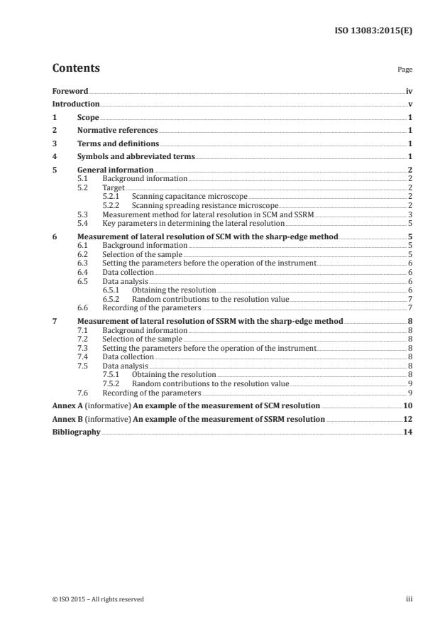
Contents Page
Foreword .iv
Introduction .v
1 Scope . 1
2 Normative references . 1
3 Terms and definitions . 1
4 Symbols and abbreviated terms . 1
5 General information . 2
5.1 Background information . 2
5.2 Target . 2
5.2.1 Scanning capacitance microscope . 2
5.2.2 Scanning spreading resistance microscope . 2
5.3 Measurement method for lateral resolution in SCM and SSRM . 3
5.4 Key parameters in determining the lateral resolution . 5
6 Measurement of lateral resolution of SCM with the sharp-edge method .5
6.1 Background information . 5
6.2 Selection of the sample . 5
6.3 Setting the parameters before the operation of the instrument . 6
6.4 Data collection . 6
6.5 Data analysis . 6
6.5.1 Obtaining the resolution . 6
6.5.2 Random contributions to the resolution value . 7
6.6 Recording of the parameters . 7
7 Measurement of lateral resolution of SSRM with the sharp-edge method .8
7.1 Background information . 8
7.2 Selection of the sample . 8
7.3 Setting the parameters before the operation of the instrument . 8
7.4 Data collection . 8
7.5 Data analysis . 8
7.5.1 Obtaining the resolution . 8
7.5.2 Random contributions to the resolution value . 9
7.6 Recording of the parameters . 9
Annex A (informative) An example of the measurement of SCM resolution .10
Annex B (informative) An example of the measurement of SSRM resolution .12
Bibliography .14
Foreword
ISO (the International Organization for Standardization) is a worldwide federation of national standards
bodies (ISO member bodies). The work of preparing International Standards is normally carried out
through ISO technical committees. Each member body interested in a subject for which a technical
committee has been established has the right to be represented on that committee. International
organizations, governmental and non-governmental, in liaison with ISO, also take part in the work.
ISO collaborates closely with the International Electrotechnical Commission (IEC) on all matters of
electrotechnical standardization.
The procedures used to develop this document and those intended for its further maintenance are
described in the ISO/IEC Directives, Part 1. In particular the different approval criteria needed for the
different types of ISO documents should be noted. This document was drafted in accordance with the
editorial rules of the ISO/IEC Directives, Part 2 (see www.iso.org/directives).
Attention is drawn to the possibility that some of the elements of this document may be the subject of
patent rights. ISO shall not be held responsible for identifying any or all such patent rights. Details of
any patent rights identified during the development of the document will be in the Introduction and/or
on the ISO list of patent declarations received (see www.iso.org/patents).
Any trade name used in this document is information given for the convenience of users and does not
constitute an endorsement.
For an explanation on the meaning of ISO specific terms and expressions related to conformity
assessment, as well as information about ISO’s adherence to the WTO principles in the Technical
Barriers to Trade (TBT) see the following URL: Foreword - Supplementary information
The committee responsible for this document is ISO/TC 201, Surface chemical analysis, Subcommittee
SC 9, Scanning probe microscopy.
iv © ISO 2015 – All rights reserved
Introduction
Electrical scanning probe microscopy (ESPM) is a branch of scanning probe microscopy (SPM) with
the capability of electrical imaging at nanometre spatial resolution. ESPM includes electrostatic force
microscopy (EFM), scanning capacitance microscopy (SCM), scanning spreading resistance microscopy
(SSRM), etc. Because ESPM can observe electrical or electronic properties with molecule-scale
resolution, it is applied to many fields such as semiconductors, displays, etc. However, there has been no
standard measurement method for the spatial resolution.
In this International Standard, standardized procedures to determine the spatial (lateral) resolution
of SSRM and SCM, which are widely used to image the distribution of carrier and other electrical
properties in semiconductor devices, are provided with the use of suitable reference materials. This
International Standard uses the sharp-edge method to measure the lateral resolution of ESPM in a
similar manner to that already used in measuring the resolution in micro-beam spectroscopy and in
depth-profiling measurements with Auger electron spectroscopy and X-ray photoelectron spectroscopy
(refer to ISO 18516).
INTERNATIONAL STANDARD ISO 13083:2015(E)
Surface chemical analysis — Scanning probe microscopy
— Standards on the definition and calibration of spatial
resolution of electrical scanning probe microscopes
(ESPMs) such as SSRM and SCM for 2D-dopant imaging and
other purposes
1 Scope
This International Standard describes a method for measuring the spatial (lateral) resolution of
scanning capacitance microscopes (SCMs) or scanning spreading resistance microscopes (SSRMs),
which are widely used in imaging the distribution of carriers and other electrical properties in
semiconductor devices. The method involves the use of a sharp-edged artefact.
2 Normative references
The following documents, in whole or in part, are normatively referenced in this document and are
indispensable for its application. For dated references, only the edition cited applies. For undated
references, the latest edition of the referenced document (including any amendments) applies.
ISO 18115-2, Surface chemical analysis – Vocabulary – Part 2: Terms used in scanning-probe microscopy
3 Terms and definitions
For the purposes of this document, the terms and definitions given in ISO 18115-2 and the following apply.
3.1
electrical scanning probe microscopy
ESPM
SPM mode in which a conductive tip is used to measure electrical properties such as capacitance,
resistance, electrical field, etc.
3.2
contact mode
mode of scanning the probe tip over the sample surface, adjusting the relative heights of the probe and
sample, in which there is always a repulsive force between the probe and the sample
Note 1 to entry: This mode can be, for example, either the constant-height or constant-force mode.
[SOURCE: ISO 18115-2:2013, 6.35]
4 Symbols and abbreviated terms
AC alternating current
DC direct current
ESPM electrical scanning probe microscopy
SPM scanning probe microscopy
AFM atomic force microscopy
MIS metal-insulator-semiconductor
MOS metal-oxide-semiconductor
SCM scanning capacitance microscopy
SIMS secondary ion mass spectroscopy
S/N signal to noise ratio
SSRM scanning spreading resistance microscopy
TEM transmission electron microscope
2D two dimension
Δx spatial resolution of ESPM
5 General information
5.1 Background information
ESPM is a branch of scanning probe microscope that can be used to image an electrical or electronic
property of a sample surface using an electrically conducting probe. Since this conductive probe is
scanned over the sample surface in the contact mode, its lateral resolution is strongly related to the
size and shape of the probe apex. Currently, this can be as small as a few nanometres, enabling sub-10
nanometre spatial resolution to be achieved. Such a high resolution, shown in ESPM images, allows the
investigation of the two-dimensional distribution of carriers in nanoscale semiconductor devices.
5.2 Target
There are a number of types of ESPM categorized by the methods of electrical characterization. Among
these ESPMs, this International Standard is for SCM and SSRM.
5.2.1 Scanning capacitance microscope
Scanning capacitance microscopy (SCM) is a modification of scanning probe microscopy in which a
conductive probe is in contact with the surface of a sample, with an applied AC bias, and scanned across
it. SCM characterizes the change in electrostatic capacitance between the sample and the probe on
the surface of the sample. SCM uses an ultra-sharp conducting probe made from etched silicon (often
coated with Pt/Ir or Co/Cr alloy) to form a metal-insulator-semiconductor (MIS/MOS) capacitor with a
semiconductor sample if a native oxide exists on the sample. When the conducting probe is in contact
to the surface under an AC bias, generated capacitance variations on the surface can be detected using
a GHz resonant capacitance sensor. The probe is then scanned across the semiconductor’s surface in x-
and y-axes while the probe is operated under the contact mode.
By applying an alternating bias to the metal-coated probe or the sample, carriers are alternately
accumulated and depleted within the semiconductor’s surface layers under the probe, changing the
tip-sample capacitance. The magnitude of this change in capacitance with the applied voltage gives
information about the concentration of carriers (SCM amplitude data), whereas the difference in phase
between the capacitance change and the applied, alternating bias carries information about the sign of
[2]
the charge carriers (SCM phase data).
5.2.2 Scanning spreading resistance microscope
A very challenging task as the size of the semiconductor components shrinks towards sub-100 nm
level is the development of new tools allowing two-dimensional (2D) carrier profiling with very high
spatial resolution. One of the promising new tools is scanning spreading resistance microscopy (SSRM).
2 © ISO 2015 – All rights reserved
SSRM is based on atomic force microscopy (AFM) and has been developed in recent years to probe
the 2D resistivity and carrier distribution in semiconductor devices. In SSRM, a very small conductive
tip is contacted on the sample surface to be used to measure the local spreading resistance, which is
intimately linked to the local resistivity. Scanning a cross section of the sample provides a 2D map of
the local spreading resistance with a spatial resolution set by the tip radius (typically 5 nm ~ 15 nm).
The main advantages of SSRM lie in its relative robustness, as it is less sensitive to surface preparation
than, for instance, scanning capacitance microscopy (SCM) leading to excellent reproducibility.
SSRM also benefits from an excellent dynamic range covering the entire dopant range of interest
14 20 −3
(10 ~ 10 ) cm with constant sensitivity and from a high spatial resolution (set by the tip radius
[3]
only) combined with very accurate junction delineation capabilities.
5.3 Measurement method for lateral resolution in SCM and SSRM
The spatial resolution is not only influenced by geometric factors of the conductive probe. Other factors
that affect spatial resolution include surface roughness of the sample, contrast of the electrical image
from difference in carrier density, pixilation, noise and sensitivity of the detector. The spatial resolution
of the ESPM instrument or the image has been determined by a few methods: imaging a regular pattern
and measuring the smallest feature and imaging across an electrically abrupt interface, etc.
It is very difficult to fabricate electrically separated layers with two different carrier density. Also, it is
crucial to connect, electrically, each plane of the repetitive pattern or the smallest feature. Therefore,
the method chosen here is the sharp-edge method based on consideration of ease of use. This method of
resolution definition is widely applied for depth-profiling of micro-beam spectroscopy such as secondary
ion mass spectroscopy (SIMS). An electrically abrupt interface is line-scanned perpendicularly across
the interface by a conductive probe and the detected profile of electrical characteristics is inspected.
In the micro-beam spectroscopy, so called 16 % to 84 % width or some other criterion may be applied
[1][4]
as the spatial resolution of SCM or SSRM as shown in Figure 1. However, the definition of the
resolution as 10 % to 90 % width is adopted as a standard method for SCM and SSRM since it has been
[5][6]
well agreed academically.
a) Side view of the sample and probe
Δx
b) Electric output as a function of the scan position
Key
1 conductive probe
2 coating
3 silicon
Δx spatial resolution of ESPM
Figure 1 — Schematic of sharp-edge method applied to SCM and SSRM
In applying this method and to obtain high-resolution data, the following should be noted.
a) It is recognized that in SSRM, the resolution depends on the contrast. Therefore, the resolution
should be compared at the same contrast level. A discussion of contrast levels is given in 7.3.
b) The resolution is also a result of mechanical probe-sample contact between the sample and probe.
The mechanical probe condition and the mechanical contact may change continuously even for a
good contact mode. In general, the probe apex shape, outer metal coating condition and the contact
area continuously change, causing the signal to fluctuate. Also, the electrical property of the silicon
or its coating will not be perfectly uniform. These inhomogeneities may increase the noise and
uncertainty levels. Therefore, the property of calibration sample, the experimental condition, and
the S/N ratio should be considered carefully to obtain the optimum result.
4 © ISO 2015 – All rights reserved
5.4 Key parameters in determining the lateral resolution
The measurement of lateral resolution can depend upon a number of experimental factors. They could
be physical properties of the SCM or SSRM instrument and the sample surface, such as the conductive
probe condition and the surface roughness. The following are the most important:
a) apex size of conductive probe: The apex size of the conductive probe is the most determining factor.
Smaller
...


Questions, Comments and Discussion
Ask us and Technical Secretary will try to provide an answer. You can facilitate discussion about the standard in here.
Loading comments...