ASTM F1467-18
(Guide)Standard Guide for Use of an X-Ray Tester (≈10 keV Photons) in Ionizing Radiation Effects Testing of Semiconductor Devices and Microcircuits
Standard Guide for Use of an X-Ray Tester (≈10 keV Photons) in Ionizing Radiation Effects Testing of Semiconductor Devices and Microcircuits
SIGNIFICANCE AND USE
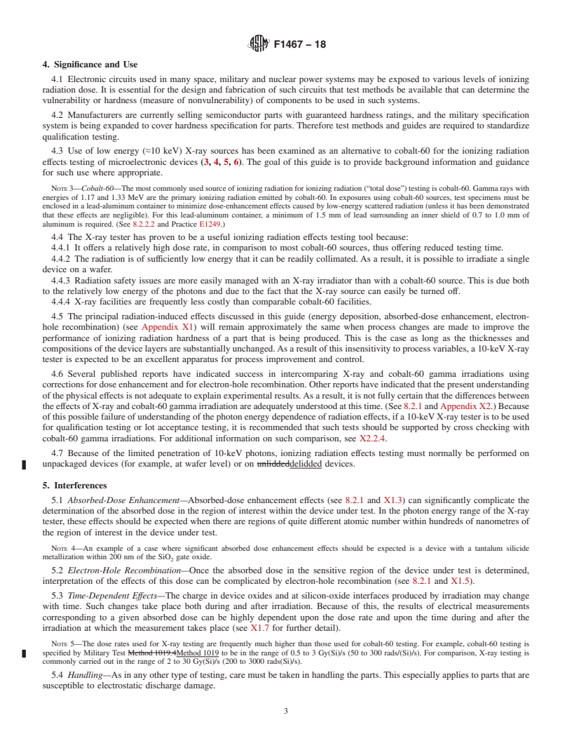
4.1 Electronic circuits used in many space, military and nuclear power systems may be exposed to various levels of ionizing radiation dose. It is essential for the design and fabrication of such circuits that test methods be available that can determine the vulnerability or hardness (measure of nonvulnerability) of components to be used in such systems.
4.2 Manufacturers are currently selling semiconductor parts with guaranteed hardness ratings, and the military specification system is being expanded to cover hardness specification for parts. Therefore test methods and guides are required to standardize qualification testing.
4.3 Use of low energy (≈10 keV) X-ray sources has been examined as an alternative to cobalt-60 for the ionizing radiation effects testing of microelectronic devices (3, 4, 5, 6). The goal of this guide is to provide background information and guidance for such use where appropriate.
Note 3: Cobalt-60—The most commonly used source of ionizing radiation for ionizing radiation (“total dose”) testing is cobalt-60. Gamma rays with energies of 1.17 and 1.33 MeV are the primary ionizing radiation emitted by cobalt-60. In exposures using cobalt-60 sources, test specimens must be enclosed in a lead-aluminum container to minimize dose-enhancement effects caused by low-energy scattered radiation (unless it has been demonstrated that these effects are negligible). For this lead-aluminum container, a minimum of 1.5 mm of lead surrounding an inner shield of 0.7 to 1.0 mm of aluminum is required. (See 8.2.2.2 and Practice E1249.)
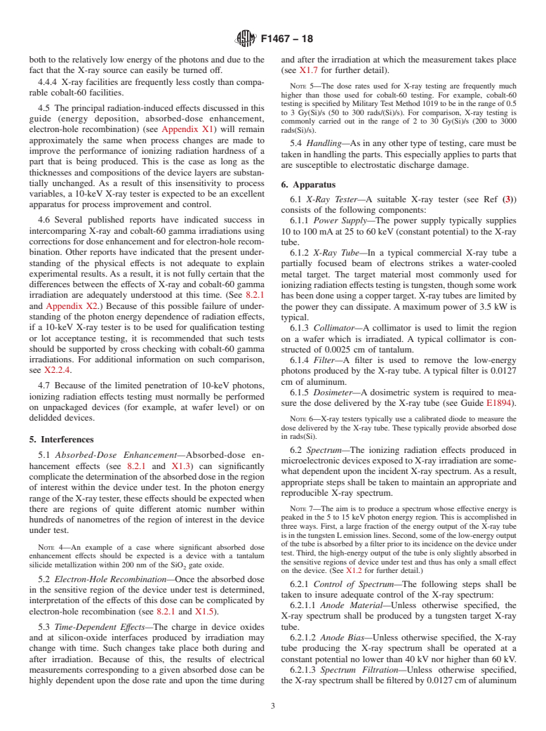
4.4 The X-ray tester has proven to be a useful ionizing radiation effects testing tool because:
4.4.1 It offers a relatively high dose rate, in comparison to most cobalt-60 sources, thus offering reduced testing time.
4.4.2 The radiation is of sufficiently low energy that it can be readily collimated. As a result, it is possible to irradiate a single device on a wafer.
4.4.3 Radiation safety issues are more easily...
SCOPE
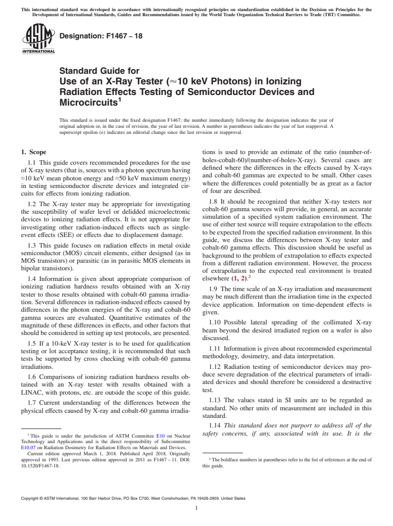
1.1 This guide covers recommended procedures for the use of X-ray testers (that is, sources with a photon spectrum having ≈10 keV mean photon energy and ≈50 keV maximum energy) in testing semiconductor discrete devices and integrated circuits for effects from ionizing radiation.
1.2 The X-ray tester may be appropriate for investigating the susceptibility of wafer level or delidded microelectronic devices to ionizing radiation effects. It is not appropriate for investigating other radiation-induced effects such as single-event effects (SEE) or effects due to displacement damage.
1.3 This guide focuses on radiation effects in metal oxide semiconductor (MOS) circuit elements, either designed (as in MOS transistors) or parasitic (as in parasitic MOS elements in bipolar transistors).
1.4 Information is given about appropriate comparison of ionizing radiation hardness results obtained with an X-ray tester to those results obtained with cobalt-60 gamma irradiation. Several differences in radiation-induced effects caused by differences in the photon energies of the X-ray and cobalt-60 gamma sources are evaluated. Quantitative estimates of the magnitude of these differences in effects, and other factors that should be considered in setting up test protocols, are presented.
1.5 If a 10-keV X-ray tester is to be used for qualification testing or lot acceptance testing, it is recommended that such tests be supported by cross checking with cobalt-60 gamma irradiations.
1.6 Comparisons of ionizing radiation hardness results obtained with an X-ray tester with results obtained with a LINAC, with protons, etc. are outside the scope of this guide.
1.7 Current understanding of the differences between the physical effects caused by X-ray and cobalt-60 gamma irradiations is used to provide an estimate of the ratio (number-of-holes-cobalt-60)/(number-of-holes-X-ray). Several cases are defined where the differences in the eff...
General Information
Relations
Buy Standard
Standards Content (Sample)
This international standard was developed in accordance with internationally recognized principles on standardization established in the Decision on Principles for the
Development of International Standards, Guides and Recommendations issued by the World Trade Organization Technical Barriers to Trade (TBT) Committee.
Designation: F1467 − 18
Standard Guide for
Use of an X-Ray Tester ('10 keV Photons) in Ionizing
Radiation Effects Testing of Semiconductor Devices and
1
Microcircuits
This standard is issued under the fixed designation F1467; the number immediately following the designation indicates the year of
original adoption or, in the case of revision, the year of last revision. A number in parentheses indicates the year of last reapproval. A
superscript epsilon (´) indicates an editorial change since the last revision or reapproval.
1. Scope tions is used to provide an estimate of the ratio (number-of-
holes-cobalt-60)/(number-of-holes-X-ray). Several cases are
1.1 This guide covers recommended procedures for the use
defined where the differences in the effects caused by X-rays
of X-ray testers (that is, sources with a photon spectrum having
and cobalt-60 gammas are expected to be small. Other cases
≈10 keV mean photon energy and ≈50 keV maximum energy)
where the differences could potentially be as great as a factor
in testing semiconductor discrete devices and integrated cir-
of four are described.
cuits for effects from ionizing radiation.
1.8 It should be recognized that neither X-ray testers nor
1.2 The X-ray tester may be appropriate for investigating
cobalt-60 gamma sources will provide, in general, an accurate
the susceptibility of wafer level or delidded microelectronic
simulation of a specified system radiation environment. The
devices to ionizing radiation effects. It is not appropriate for
use of either test source will require extrapolation to the effects
investigating other radiation-induced effects such as single-
to be expected from the specified radiation environment. In this
event effects (SEE) or effects due to displacement damage.
guide, we discuss the differences between X-ray tester and
1.3 This guide focuses on radiation effects in metal oxide
cobalt-60 gamma effects. This discussion should be useful as
semiconductor (MOS) circuit elements, either designed (as in
background to the problem of extrapolation to effects expected
MOS transistors) or parasitic (as in parasitic MOS elements in
from a different radiation environment. However, the process
bipolar transistors).
of extrapolation to the expected real environment is treated
2
1.4 Information is given about appropriate comparison of elsewhere (1, 2).
ionizing radiation hardness results obtained with an X-ray
1.9 The time scale of an X-ray irradiation and measurement
tester to those results obtained with cobalt-60 gamma irradia-
may be much different than the irradiation time in the expected
tion. Several differences in radiation-induced effects caused by
device application. Information on time-dependent effects is
differences in the photon energies of the X-ray and cobalt-60
given.
gamma sources are evaluated. Quantitative estimates of the
1.10 Possible lateral spreading of the collimated X-ray
magnitude of these differences in effects, and other factors that
beam beyond the desired irradiated region on a wafer is also
should be considered in setting up test protocols, are presented.
discussed.
1.5 If a 10-keV X-ray tester is to be used for qualification
1.11 Information is given about recommended experimental
testing or lot acceptance testing, it is recommended that such
methodology, dosimetry, and data interpretation.
tests be supported by cross checking with cobalt-60 gamma
irradiations. 1.12 Radiation testing of semiconductor devices may pro-
duce severe degradation of the electrical parameters of irradi-
1.6 Comparisons of ionizing radiation hardness results ob-
ated devices and should therefore be considered a destructive
tained with an X-ray tester with results obtained with a
test.
LINAC, with protons, etc. are outside the scope of this guide.
1.13 The values stated in SI units are to be regarded as
1.7 Current understanding of the differences between the
standard. No other units of measurement are included in this
physical effects caused by X-ray and cobalt-60 gamma irradia-
standard.
1.14 This standard does not purport to address all of the
safety concerns, if any, associated with its use. It is the
1
This guide is under the jurisdiction of ASTM Committee E10 on Nuclear
Technology and Applications and is the direct responsibility of Subcommittee
E10.07 on Radiation Dosimetry for Radiation Effects on Materials and Devices.
Current edition approved March 1, 2018. Published April 2018. Originally
2
approved in 1993. Last previous edition approved in 2011 as F1467 – 11. DOI: The boldface numbers in parentheses refer to the list of references at the end of
10.1520/F1467-18. this guide.
Copyright © ASTM International, 100 Barr Ha
...
This document is not an ASTM standard and is intended only to provide the user of an ASTM standard an indication of what changes have been made to the previous version. Because
it may not be technically possible to adequately depict all changes accurately, ASTM recommends that users consult prior editions as appropriate. In all cases only the current version
of the standard as published by ASTM is to be considered the official document.
Designation: F1467 − 11 F1467 − 18
Standard Guide for
Use of an X-Ray Tester ('10 keV Photons) in Ionizing
Radiation Effects Testing of Semiconductor Devices and
1
Microcircuits
This standard is issued under the fixed designation F1467; the number immediately following the designation indicates the year of
original adoption or, in the case of revision, the year of last revision. A number in parentheses indicates the year of last reapproval. A
superscript epsilon (´) indicates an editorial change since the last revision or reapproval.
1. Scope
1.1 This guide covers recommended procedures for the use of X-ray testers (that is, sources with a photon spectrum having ≈10
keV mean photon energy and ≈50 keV maximum energy) in testing semiconductor discrete devices and integrated circuits for
effects from ionizing radiation.
1.2 The X-ray tester may be appropriate for investigating the susceptibility of wafer level or delidded microelectronic devices
to ionizing radiation effects. It is not appropriate for investigating other radiation-induced effects such as single-event effects (SEE)
or effects due to displacement damage.
1.3 This guide focuses on radiation effects in metal oxide semiconductor (MOS) circuit elements, either designed (as in MOS
transistors) or parasitic (as in parasitic MOS elements in bipolar transistors).
1.4 Information is given about appropriate comparison of ionizing radiation hardness results obtained with an X-ray tester to
those results obtained with cobalt-60 gamma irradiation. Several differences in radiation-induced effects caused by differences in
the photon energies of the X-ray and cobalt-60 gamma sources are evaluated. Quantitative estimates of the magnitude of these
differences in effects, and other factors that should be considered in setting up test protocols, are presented.
1.5 If a 10-keV X-ray tester is to be used for qualification testing or lot acceptance testing, it is recommended that such tests
be supported by cross checking with cobalt-60 gamma irradiations.
1.6 Comparisons of ionizing radiation hardness results obtained with an X-ray tester with results obtained with a LINAC, with
protons, etc. are outside the scope of this guide.
1.7 Current understanding of the differences between the physical effects caused by X-ray and cobalt-60 gamma irradiations is
used to provide an estimate of the ratio (number-of-holes-cobalt-60)/(number-of-holes-X-ray). Several cases are defined where the
differences in the effects caused by X-rays and cobalt-60 gammas are expected to be small. Other cases where the differences could
potentially be as great as a factor of four are described.
1.8 It should be recognized that neither X-ray testers nor cobalt-60 gamma sources will provide, in general, an accurate
simulation of a specified system radiation environment. The use of either test source will require extrapolation to the effects to be
expected from the specified radiation environment. In this guide, we discuss the differences between X-ray tester and cobalt-60
gamma effects. This discussion should be useful as background to the problem of extrapolation to effects expected from a different
2
radiation environment. However, the process of extrapolation to the expected real environment is treated elsewhere (1, 2).
1.9 The time scale of an X-ray irradiation and measurement may be much different than the irradiation time in the expected
device application. Information on time-dependent effects is given.
1.10 Possible lateral spreading of the collimated X-ray beam beyond the desired irradiated region on a wafer is also discussed.
1.11 Information is given about recommended experimental methodology, dosimetry, and data interpretation.
1.12 Radiation testing of semiconductor devices may produce severe degradation of the electrical parameters of irradiated
devices and should therefore be considered a destructive test.
1
This guide is under the jurisdiction of ASTM Committee F01 on Electronicsand is the direct responsibility of Subcommittee F01.11 on Nuclear and Space Radiation
Effects.
Current edition approved Oct. 1, 2011March 1, 2018. Published October 2011April 2018. Originally approved in 1993. Last previous edition approved in 20052011 as
ε1
F1467 - 99F1467 - 11.(2005) . DOI: 10.1520/F1467-11.10.1520/F1467-18.
2
The boldface numbers in parentheses refer to the list of references at the end of this guide.
Copyright © ASTM International, 100 Barr Harbor Drive, PO Box C700, West Conshohocken, PA 19428-2959. United States
1
---------------------- Page: 1 --------
...


Questions, Comments and Discussion
Ask us and Technical Secretary will try to provide an answer. You can facilitate discussion about the standard in here.