ASTM E983-10(2018)
(Guide)Standard Guide for Minimizing Unwanted Electron Beam Effects in Auger Electron Spectroscopy
Standard Guide for Minimizing Unwanted Electron Beam Effects in Auger Electron Spectroscopy
SIGNIFICANCE AND USE
4.1 When electron beam excitation is used in AES, the incident electron beam can interact with the specimen material causing physical and chemical changes. In general, these effects are a hindrance to AES analysis because they cause localized specimen modification (1-4).4
4.2 With specimens that have poor electrical conductivity the electron beam can stimulate the development of localized charge on the specimen surface. This effect is a hindrance to AES analysis because the potentials associated with the charge can either adversely affect the integrity of Auger data or make Auger data collection difficult (5, 6).
SCOPE
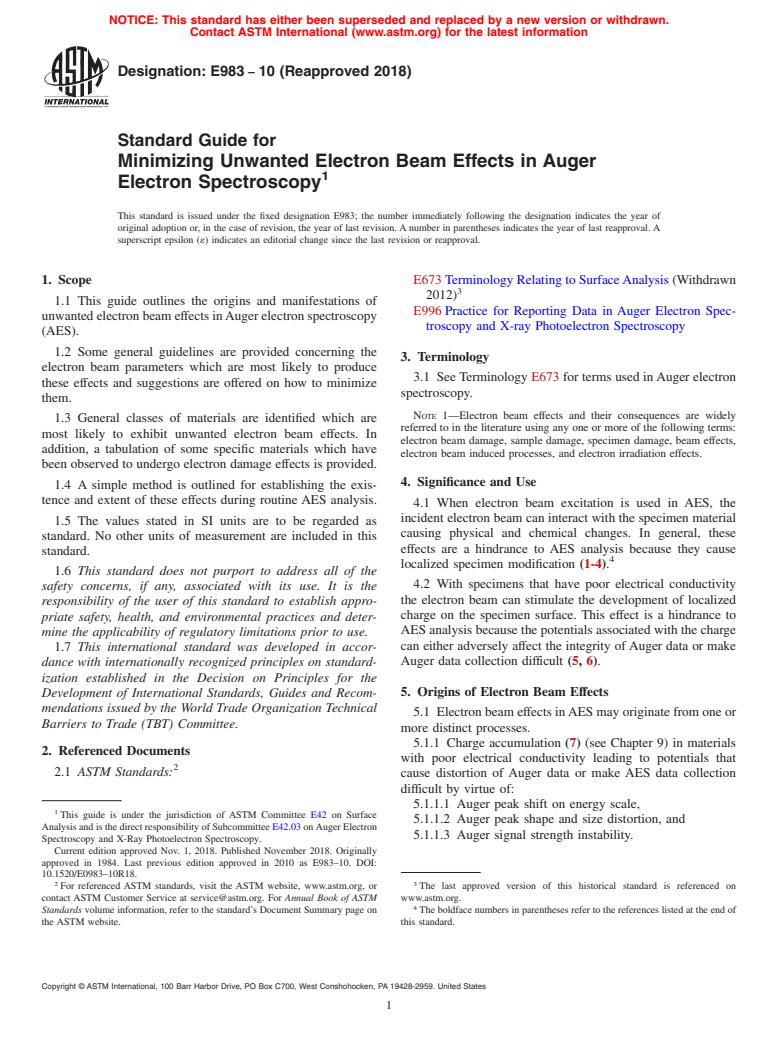
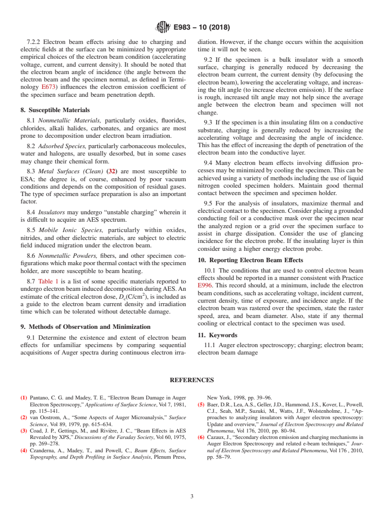
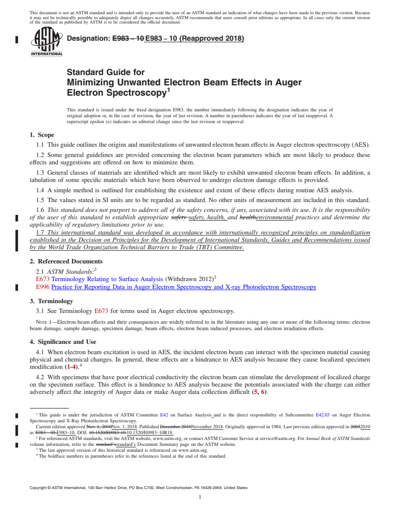
1.1 This guide outlines the origins and manifestations of unwanted electron beam effects in Auger electron spectroscopy (AES).
1.2 Some general guidelines are provided concerning the electron beam parameters which are most likely to produce these effects and suggestions are offered on how to minimize them.
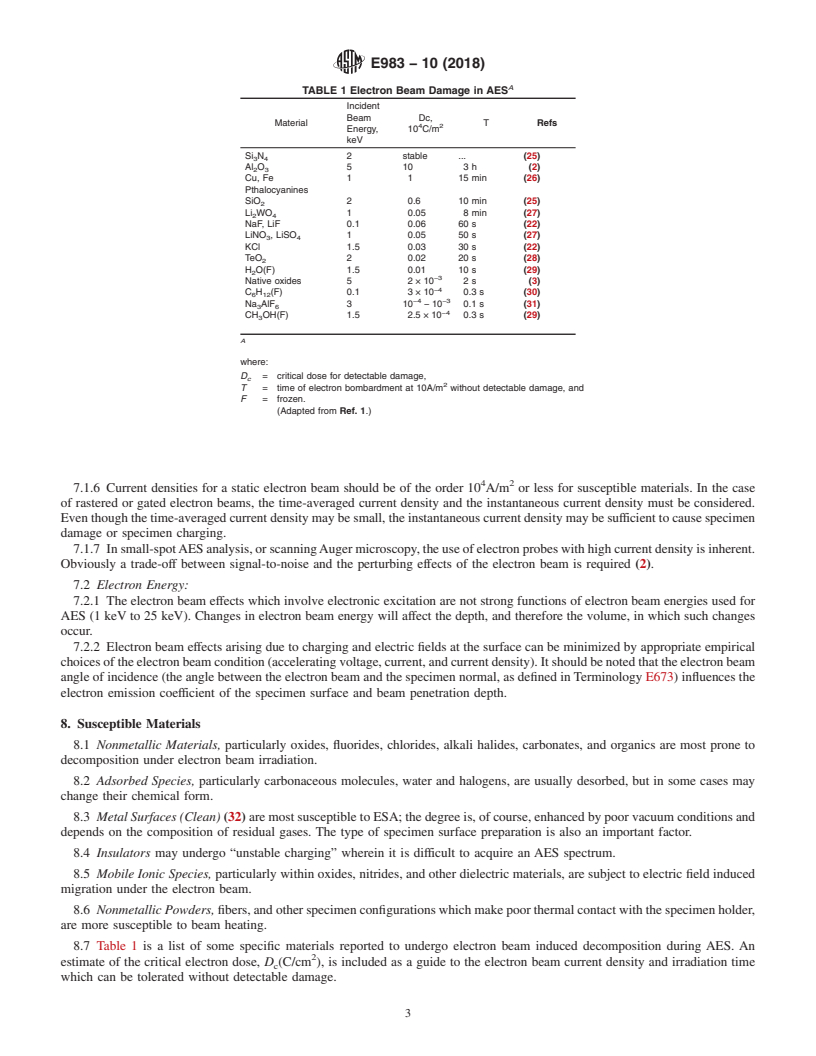
1.3 General classes of materials are identified which are most likely to exhibit unwanted electron beam effects. In addition, a tabulation of some specific materials which have been observed to undergo electron damage effects is provided.
1.4 A simple method is outlined for establishing the existence and extent of these effects during routine AES analysis.
1.5 The values stated in SI units are to be regarded as standard. No other units of measurement are included in this standard.
1.6 This standard does not purport to address all of the safety concerns, if any, associated with its use. It is the responsibility of the user of this standard to establish appropriate safety, health, and environmental practices and determine the applicability of regulatory limitations prior to use.
1.7 This international standard was developed in accordance with internationally recognized principles on standardization established in the Decision on Principles for the Development of International Standards, Guides and Recommendations issued by the World Trade Organization Technical Barriers to Trade (TBT) Committee.
General Information
Relations
Buy Standard
Standards Content (Sample)
NOTICE: This standard has either been superseded and replaced by a new version or withdrawn.
Contact ASTM International (www.astm.org) for the latest information
Designation: E983 − 10 (Reapproved 2018)
Standard Guide for
Minimizing Unwanted Electron Beam Effects in Auger
Electron Spectroscopy
This standard is issued under the fixed designation E983; the number immediately following the designation indicates the year of
original adoption or, in the case of revision, the year of last revision. A number in parentheses indicates the year of last reapproval. A
superscript epsilon (´) indicates an editorial change since the last revision or reapproval.
1. Scope E673 Terminology Relating to SurfaceAnalysis (Withdrawn
2012)
1.1 This guide outlines the origins and manifestations of
E996 Practice for Reporting Data in Auger Electron Spec-
unwanted electron beam effects inAuger electron spectroscopy
troscopy and X-ray Photoelectron Spectroscopy
(AES).
1.2 Some general guidelines are provided concerning the
3. Terminology
electron beam parameters which are most likely to produce
3.1 See Terminology E673 for terms used inAuger electron
these effects and suggestions are offered on how to minimize
spectroscopy.
them.
NOTE 1—Electron beam effects and their consequences are widely
1.3 General classes of materials are identified which are
referred to in the literature using any one or more of the following terms:
most likely to exhibit unwanted electron beam effects. In
electron beam damage, sample damage, specimen damage, beam effects,
addition, a tabulation of some specific materials which have
electron beam induced processes, and electron irradiation effects.
been observed to undergo electron damage effects is provided.
4. Significance and Use
1.4 A simple method is outlined for establishing the exis-
tence and extent of these effects during routine AES analysis.
4.1 When electron beam excitation is used in AES, the
incident electron beam can interact with the specimen material
1.5 The values stated in SI units are to be regarded as
causing physical and chemical changes. In general, these
standard. No other units of measurement are included in this
effects are a hindrance to AES analysis because they cause
standard.
localized specimen modification (1-4).
1.6 This standard does not purport to address all of the
4.2 With specimens that have poor electrical conductivity
safety concerns, if any, associated with its use. It is the
the electron beam can stimulate the development of localized
responsibility of the user of this standard to establish appro-
charge on the specimen surface. This effect is a hindrance to
priate safety, health, and environmental practices and deter-
AES analysis because the potentials associated with the charge
mine the applicability of regulatory limitations prior to use.
can either adversely affect the integrity of Auger data or make
1.7 This international standard was developed in accor-
Auger data collection difficult (5, 6).
dance with internationally recognized principles on standard-
ization established in the Decision on Principles for the
5. Origins of Electron Beam Effects
Development of International Standards, Guides and Recom-
mendations issued by the World Trade Organization Technical
5.1 Electron beam effects inAES may originate from one or
Barriers to Trade (TBT) Committee.
more distinct processes.
5.1.1 Charge accumulation (7) (see Chapter 9) in materials
2. Referenced Documents
with poor electrical conductivity leading to potentials that
2.1 ASTM Standards:
cause distortion of Auger data or make AES data collection
difficult by virtue of:
5.1.1.1 Auger peak shift on energy scale,
This guide is under the jurisdiction of ASTM Committee E42 on Surface
5.1.1.2 Auger peak shape and size distortion, and
Analysis and is the direct responsibility of Subcommittee E42.03 on Auger Electron
5.1.1.3 Auger signal strength instability.
Spectroscopy and X-Ray Photoelectron Spectroscopy.
Current edition approved Nov. 1, 2018. Published November 2018. Originally
approved in 1984. Last previous edition approved in 2010 as E983–10. DOI:
10.1520/E0983–10R18.
2 3
For referenced ASTM standards, visit the ASTM website, www.astm.org, or The last approved version of this historical standard is referenced on
contact ASTM Customer Service at service@astm.org. For Annual Book of ASTM www.astm.org.
Standards volume information, refer to the standard’s Document Summary page on The boldface numbers in parentheses refer to the references listed at the end of
the ASTM website. this standard.
Copyright © ASTM International, 100 Barr Harbor Drive, PO Box C700, West Conshohocken, PA 19428-2959. United States
E983 − 10 (2018)
A
TABLE 1 Electron Beam Damage in AES
5.1.2 Electronic excitation of surface, subsurface, and bulk
Incident
atoms and molecules leading to specimen changes (8-10)
Beam Dc,
which include: Material T Refs
4 2
Energy, 10 C/m
5.1.2.1 Dissociation,
keV
5.1.2.2 Electron stimulated desorption (ESD) (11),
Si N 2 stable . (25)
3 4
Al O 5103h (2)
2 3
5.1.2.3 Electron stimulated adsorption (ESA) (12),
Cu, Fe 1 1 15 min (26)
5.1.2.4 Polymerization (13, 14),
Pthalocyanines
5.1.2.5 Carburization (15-17), SiO 2 0.6 10 min (25)
Li WO 1 0.05 8 min (27)
5.1.2.6 Oxidation (18, 19), 2 4
NaF, LiF 0.1 0.06 60 s (22)
5.1.2.7 Reduction (20),
LiNO , LiSO 10.05 50s (27)
3 4
5.1.2.8 Decomposition (21, 22),
KCl 1.5 0.03 30 s (22)
TeO 20.02 20s (28)
5.1.2.9 Erosion, and
H O(F) 1.5 0.01 10 s (29)
5.1.2.10 Diffusion.
−3
Native oxides 5 2 × 10 2s (3)
−4
5.1.3 Charge accumulation in materials of poor electrical C H (F) 0.1 3 × 10 0.3 s (30)
6 12
−4 −3
Na AlF 310 −10 0.1 s (31)
3 6
conductivity leading to specimen changes which include (23,
−4
CH OH(F) 1.5 2.5 × 10 0.3 s (29)
24, 7) (see Chapter 8):
5.1.3.1 Electric field enhanced diffusion, and
A
5.1.3.2 Electromigration (4) (see p. 62).
where:
5.1.4 Heating which may cause:
D = critical dose for detectable damage,
c
5.1.4.1 Annealing,
T = time of electron bombardment at 10A/m without detectable damage, and
5.1.4.2 Segregation, F = frozen.
(Adapted from Ref. 1.)
5.1.4.3 Volatilization, and
5.1.4.4 Chemical reaction.
6. Practical Manifestations of Electron Beam Effects
a material specific critical dose, D . The magnitude of the
c
6.1 Electron dose dependent changes in the intensity,
critical dose corresponds to the onset of detectable damage and
energy, or peak shape of one or moreAuger transitions, or any
the values may be subject to future revision. The material
combination thereof; depending upon the material, these
specific critical dose, D , may be as low as 1 C⁄m .
c
changes may be complete within a fraction of a second or they
7.1.4 In practice, the electron dose is directly dependent
may progress for hours.
upon the electron beam current density, J , (A/m ), the time of
B
electron irradiation in seconds, t(s); and the angle of incidence,
6.2 Discoloration of the specimen in the proximity of the
2 2
Θ, of the beam on the sample. That is, D (C/m )= J (A/m
electron beam irradiated region.
C B
)·t(s)·cosΘ. Using a typical electron beam current density,
6.3 Physical damage to the specimen such as erosion,
2 -8
10 A⁄m would be equivalent to using 10 A incident beam
cracking, blistering, or densification.
current into a 33 µm electron beam diameter at normal
6.4 Pressure rises in the analytical vacuum chamber during
incidence.
electron irradiation.
7.1.5 Theelectronbeam-inducedheatingofagivenmaterial
of poor thermal conductivity and the accumulation of charge
6.5 Localized electric charge dependent changes in the
on a material of poor electrical conductivity are dependent
intensity, energy, or peak shape of allAuger transitions, or any
upon the electron beam current density.
combination thereof. These changes may be stable but often
7.1.6 Current densities for a static electron beam should be
are erratic resulting in unstable AES signals which may
4 2
of the order 10 A/m or less for susceptible materials. In the
preclude AES data collection.
case of rastered or gated electron beams, the time-averaged
7. Electron Beam Parameters current density and the instantaneous current density must be
considered. Even though the time-averaged current density
7.1 Electron Dose and Current Density:
may be small, the instantaneous current density may be
7.1.1 Electron dose and current density were previously
2 2 sufficient to cause specimen damage or specimen charging.
defined using units of C/cm and mA/cm , respectively. These
7.1.7 In small-spot AES analysis, or scanning Auger
units are not consistent with the SI system. To keep from
microscopy, the use of electron probes with high current
changing the magnitude of the numbers appearing in the
density is inherent. Obviously a trade-off between signal-to-
literature (from which Table 1 is adapted), the multipliers of
noiseandtheperturbingeffectsoftheelectronbeamisrequired
the terms are being changed. A dose of C/cm is equivalent to
4 2 2 2 (2).
10 C/m , while 1mA/cm is equivalent to 10A/m .
7.1.2 Specimenmaterialmodificationcanoftenberelatedto 7.2 Electron Energy:
the electron dose (D); that is, the number of electrons incident 7.2.1 The electron beam effects which involve electronic
on a unit area of the specimen, expressed in coulombs per excitation are not strong functions of electron beam energies
square centimeter (C/cm ) (1). used for AES (1 keV to 25 keV). Changes in electron beam
7.1.3 A number of materials, (for example, see Table 1), energywillaffectthedepth,andthereforethevolume,inwhich
exhibit dose-dependent effects when the electron dose exceeds such changes occur.
E983 − 10 (2018)
7.2.2 Electron beam effects arising due to charging and diation. However, if the change occurs within the acquisition
electric fields at the surface can be minimized by appropriate time it will not be seen.
empirical choices of the electron beam condition (accelerating
9.2 If the specimen is a bulk insulator with a smooth
voltage, current, and current density). It should be noted that
surface, charging is generally reduced by decreasing the
the electron beam angle of incidence (the angle between the
electron beam current, the current density (by defocusing the
electron beam and the specimen normal, as defined in Termi-
electron beam), lowering the accelerating voltage, and increas-
nology E673) influences the electron emission coefficient of
ing the tilt angle (to increase electron emission). If the surface
the specimen surface and beam penetration depth.
is rough, increased tilt angle may not help since the average
angle be
...
This document is not an ASTM standard and is intended only to provide the user of an ASTM standard an indication of what changes have been made to the previous version. Because
it may not be technically possible to adequately depict all changes accurately, ASTM recommends that users consult prior editions as appropriate. In all cases only the current version
of the standard as published by ASTM is to be considered the official document.
Designation: E983 − 10 E983 − 10 (Reapproved 2018)
Standard Guide for
Minimizing Unwanted Electron Beam Effects in Auger
Electron Spectroscopy
This standard is issued under the fixed designation E983; the number immediately following the designation indicates the year of
original adoption or, in the case of revision, the year of last revision. A number in parentheses indicates the year of last reapproval. A
superscript epsilon (´) indicates an editorial change since the last revision or reapproval.
1. Scope
1.1 This guide outlines the origins and manifestations of unwanted electron beam effects in Auger electron spectroscopy (AES).
1.2 Some general guidelines are provided concerning the electron beam parameters which are most likely to produce these
effects and suggestions are offered on how to minimize them.
1.3 General classes of materials are identified which are most likely to exhibit unwanted electron beam effects. In addition, a
tabulation of some specific materials which have been observed to undergo electron damage effects is provided.
1.4 A simple method is outlined for establishing the existence and extent of these effects during routine AES analysis.
1.5 The values stated in SI units are to be regarded as standard. No other units of measurement are included in this standard.
1.6 This standard does not purport to address all of the safety concerns, if any, associated with its use. It is the responsibility
of the user of this standard to establish appropriate safety safety, health, and healthenvironmental practices and determine the
applicability of regulatory limitations prior to use.
1.7 This international standard was developed in accordance with internationally recognized principles on standardization
established in the Decision on Principles for the Development of International Standards, Guides and Recommendations issued
by the World Trade Organization Technical Barriers to Trade (TBT) Committee.
2. Referenced Documents
2.1 ASTM Standards:
E673 Terminology Relating to Surface Analysis (Withdrawn 2012)
E996 Practice for Reporting Data in Auger Electron Spectroscopy and X-ray Photoelectron Spectroscopy
3. Terminology
3.1 See Terminology E673 for terms used in Auger electron spectroscopy.
NOTE 1—Electron beam effects and their consequences are widely referred to in the literature using any one or more of the following terms: electron
beam damage, sample damage, specimen damage, beam effects, electron beam induced processes, and electron irradiation effects.
4. Significance and Use
4.1 When electron beam excitation is used in AES, the incident electron beam can interact with the specimen material causing
physical and chemical changes. In general, these effects are a hindrance to AES analysis because they cause localized specimen
modification (1-4).
4.2 With specimens that have poor electrical conductivity the electron beam can stimulate the development of localized charge
on the specimen surface. This effect is a hindrance to AES analysis because the potentials associated with the charge can either
adversely affect the integrity of Auger data or make Auger data collection difficult (5, 6).
This guide is under the jurisdiction of ASTM Committee E42 on Surface Analysis and is the direct responsibility of Subcommittee E42.03 on Auger Electron
Spectroscopy and X-Ray Photoelectron Spectroscopy.
Current edition approved Nov. 1, 2010Nov. 1, 2018. Published December 2010November 2018. Originally approved in 1984. Last previous edition approved in 20052010
as E983 – 05.E983–10. DOI: 10.1520/E0983-10.10.1520/E0983–10R18.
For referenced ASTM standards, visit the ASTM website, www.astm.org, or contact ASTM Customer Service at service@astm.org. For Annual Book of ASTM Standards
volume information, refer to the standard’sstandard’s Document Summary page on the ASTM website.
The last approved version of this historical standard is referenced on www.astm.org.
The boldface numbers in parentheses refer to the references listed at the end of this standard.
Copyright © ASTM International, 100 Barr Harbor Drive, PO Box C700, West Conshohocken, PA 19428-2959. United States
E983 − 10 (2018)
5. Origins of Electron Beam Effects
5.1 Electron beam effects in AES may originate from one or more distinct processes.
5.1.1 Charge accumulation (7) (see Chapter 9) in materials with poor electrical conductivity leading to potentials that cause
distortion of Auger data or make AES data collection difficult by virtue of:
5.1.1.1 Auger peak shift on energy scale,
5.1.1.2 Auger peak shape and size distortion, and
5.1.1.3 Auger signal strength instability.
5.1.2 Electronic excitation of surface, subsurface, and bulk atoms and molecules leading to specimen changes (8-10) which
include:
5.1.2.1 Dissociation,
5.1.2.2 Electron stimulated desorption (ESD) (11),
5.1.2.3 Electron stimulated adsorption (ESA) (12),
5.1.2.4 Polymerization (13, 14),
5.1.2.5 Carburization (15-17),
5.1.2.6 Oxidation (18, 19),
5.1.2.7 Reduction (20),
5.1.2.8 Decomposition (21, 22),
5.1.2.9 Erosion, and
5.1.2.10 Diffusion.
5.1.3 Charge accumulation in materials of poor electrical conductivity leading to specimen changes which include (23, 24, 7)
(see Chapter 8):
5.1.3.1 Electric field enhanced diffusion, and
5.1.3.2 Electromigration (4) (see p. 62).
5.1.4 Heating which may cause:
5.1.4.1 Annealing,
5.1.4.2 Segregation,
5.1.4.3 Volatilization, and
5.1.4.4 Chemical reaction.
6. Practical Manifestations of Electron Beam Effects
6.1 Electron dose dependent changes in the intensity, energy, or peak shape of one or more Auger transitions, or any
combination thereof; depending upon the material, these changes may be complete within a fraction of a second or they may
progress for hours.
6.2 Discoloration of the specimen in the proximity of the electron beam irradiated region.
6.3 Physical damage to the specimen such as erosion, cracking, blistering, or densification.
6.4 Pressure rises in the analytical vacuum chamber during electron irradiation.
6.5 Localized electric charge dependent changes in the intensity, energy, or peak shape of all Auger transitions, or any
combination thereof. These changes may be stable but often are erratic resulting in unstable AES signals which may preclude AES
data collection.
7. Electron Beam Parameters
7.1 Electron Dose and Current Density:
2 2
7.1.1 Electron dose and current density were previously defined using units of C/cm and mA/cm , respectively. These units are
not consistent with the SI system. To keep from changing the magnitude of the numbers appearing in the literature (from which
2 4 2 2
Table 1 is adapted), the multipliers of the terms are being changed. A dose of C/cm is equivalent to 10 C/m , while 1mA/cm is
equivalent to 10A/m .
7.1.2 Specimen material modification can often be related to the electron dose (D); that is, the number of electrons incident on
a unit area of the specimen, expressed in coulombs per square centimeter (C/cm ) (1).
7.1.3 A number of materials, (for example, see Table 1), exhibit dose-dependent effects when the electron dose exceeds a
material specific critical dose, D . The magnitude of the critical dose corresponds to the onset of detectable damage and the values
c
may be subject to future revision. The material specific critical dose, D , may be as low as 1 C ⁄m .
c
7.1.4 In practice, the electron dose is directly dependent upon the electron beam current density, J , (A/m ), the time of electron
B
2 2
irradiation in seconds, t(s); and the angle of incidence, Θ, of the beam on the sample. That is, D (C/m ) = J (A/m )·t(s)·cosΘ.
C B
2 -8
Using a typical electron beam current density, 10 A ⁄m would be equivalent to using 10 A incident beam current into a 33 μm
electron beam diameter at normal incidence.
7.1.5 The electron beam-induced heating of a given material of poor thermal conductivity and the accumulation of charge on
a material of poor electrical conductivity are dependent upon the electron beam current density.
E983 − 10 (2018)
A
TABLE 1 Electron Beam Damage in AES
Incident
Beam Dc,
Material T Refs
4 2
Energy, 10 C/m
keV
Si N 2 stable . (25)
3 4
Al O 5 10 3 h (2)
2 3
Cu, Fe 1 1 15 min (26)
Pthalocyanines
SiO 2 0.6 10 min (25)
Li WO 1 0.05 8 min (27)
2 4
NaF, LiF 0.1 0.06 60 s (22)
LiNO , LiSO 1 0.05 50 s (27)
3 4
KCl 1.5 0.03 30 s (22)
TeO 2 0.02 20 s (28)
H O(F) 1.5 0.01 10 s (29)
−3
Native oxides 5 2 × 10 2 s (3)
−4
C H (F) 0.1 3 × 10 0.3 s (30)
6 12
−4 −3
Na AlF 3 10 − 10 0.1 s (31)
3 6
−4
CH OH(F) 1.5 2.5 × 10 0.3 s (29)
A
where:
D = critical dose for detectable damage,
c
T = time of electron bombardment at 10A/m without detectable damage, and
F = frozen.
(Adapted from Ref. 1.)
4 2
7.1.6 Current densities for a static electron beam should be of the order 10 A/m or less for susceptible materials. In the case
of rastered or gated electron beams, the time-averaged current density and the instantaneous current density must be considered.
Even though the time-averaged current density may be small, the instantaneous current density may be sufficient to cause specimen
damage or specimen charging.
7.1.7 In small-spot AES analysis, or scanning Auger microscopy, the use of electron probes with high current density is inherent.
Obviously a trade-off between signal-to-noise and the perturbing effects of the electron beam is required (2).
7.2 Electron Energy:
7.2.1 The electron beam effects which involve electronic excitation are not strong functions of electron beam energies used for
AES (1 keV to 25 keV). Changes in electron beam energy will affect the depth, and therefore the volume, in which such changes
occur.
7.2.2 Electron beam effects arising due to charging and electric fields at the surface can be minimized by appropriate empirical
choices of the electron beam condition (accelerating voltage, current, and current density). It should be noted that the electron beam
angle of incidence (the angle between the electron beam and the specimen normal, as defined in Terminology E673) influences the
electron emission coefficient of the specimen surface and beam penetration depth.
8. Susceptible Materials
8.1 Nonmetallic Materials, particularly oxides, fluorides, chlorides, alkali halides, carbonates, and organics are most prone to
decomposition under electron beam irradiation.
8.2 Adsorbed Species, particularly carbonaceous molecules, water and halogens, are usually desorbed, but in some cases may
change their chemical form.
8.3 Metal Surfaces (Clea
...


Questions, Comments and Discussion
Ask us and Technical Secretary will try to provide an answer. You can facilitate discussion about the standard in here.