IEC 60191-6-12:2002
(Main)Mechanical standardization of semiconductor devices - Part 6-12: General rules for the preparation of outline drawings of surface mounted semiconductor device packages - Design guide for fine-pitch land grid array (FLGA) - Rectangular type
Mechanical standardization of semiconductor devices - Part 6-12: General rules for the preparation of outline drawings of surface mounted semiconductor device packages - Design guide for fine-pitch land grid array (FLGA) - Rectangular type
Provides common outline drawings and dimensions for all types of structures and composed materials of fine-pitch land grid array whose terminal pitch is less than, or equal to, 0,80 mm and whose package body outline is rectangular.
General Information
- Status
- Published
- Publication Date
- 13-Jun-2002
- Technical Committee
- SC 47D - Semiconductor devices packaging
- Drafting Committee
- WG 2 - TC 47/SC 47D/WG 2
- Current Stage
- DELPUB - Deleted Publication
- Start Date
- 08-Jun-2011
- Completion Date
- 13-Feb-2026
Relations
- Effective Date
- 05-Sep-2023
Overview
IEC 60191-6-12:2002 is an International Electrotechnical Commission design guide that standardizes mechanical outline drawings for rectangular fine‑pitch land grid array (FLGA) surface‑mounted semiconductor packages. It applies to FLGA packages whose terminal pitch is ≤ 0.80 mm and whose package body outline is rectangular. The standard is part of the IEC 60191 series on mechanical standardization of semiconductor devices.
Key topics and technical requirements
- Scope and definitions: distinguishes flanged type (package body includes a flange) and real chip size type (body equals encapsulation around chip). Material classes: P‑FLGA (plastic/interposer) and C‑FLGA (ceramic).
- Allowed terminal pitches: e = 0.80, 0.65, 0.50, 0.40 mm.
- Terminal height: FLGA terminals (lands or bumps) have terminal height ≤ 100 µm.
- Primary dimensional controls: package length (D) and width (E), nominal grid matrix (MD × ME), and terminal pitch (eD / eE).
- Group 1 (mounting & interchangeability): recommends nominal package sizes, standoff/mounting heights (e.g., VFLGA 1.00, TFLGA 1.20, LFLGA 1.70, FLGA 2.00), positional centre offsets (SD, SE), and tolerances for lateral profile (v).
- Terminal geometry & tolerances:
- Terminal diameter (b) tables for C‑FLGA and P‑FLGA with min/nom/max per pitch (examples shown for e = 0.80 → C‑FLGA bnom ≈ 0.50 mm; P‑FLGA bnom ≈ 0.40 mm).
- Positional tolerance (x) (e.g., 0.08 mm for 0.80/0.65 mm pitch, 0.05 mm for 0.50/0.40 mm).
- Coplanarity (y) tolerances (e.g., 0.12 mm for 0.80 mm; 0.10 mm for 0.65 mm; 0.08 mm for 0.50/0.40 mm).
- Group 2 (mounting & gauging): overhang formulas ZD, ZE = (Dnom − (MD−1)×e)/2 and terminal land pad sizing (b on land = bmax + x).
- Outline registration: template (Table 3) for registering individual outline drawings including full matrix, staggered or peripheral X‑row matrix arrangements; D/E vs. terminal count lookup tables for different pitches.
Applications and practical value
- Standardizes mechanical outlines and footprints to enable interchangeability, consistent PCB land‑pattern design, and reliable assembly/gauging for fine‑pitch area‑array devices.
- Guides IC package designers, PCB layout engineers, surface‑mount assembly houses, component manufacturers, and test/fixturing teams on dimensional and tolerance requirements for FLGA rectangular packages.
- Useful for procurement and compliance checks where consistent mechanical specifications reduce rework, improve yield, and simplify board‑level integration.
Related standards
- IEC 60191 (all parts) - the wider series on mechanical standardization of semiconductor devices; this document relies on and complements other parts for general rules and outline drawing practices.
Keywords: IEC 60191-6-12, FLGA, fine-pitch land grid array, rectangular FLGA, surface mounted semiconductor device, outline drawings, terminal pitch, packaging tolerances.
IEC 60191-6-12:2002 - Mechanical standardization of semiconductor devices - Part 6-12: General rules for the preparation of outline drawings of surface mounted semiconductor device packages - Design guide for fine-pitch land grid array (FLGA) - Rectangular type Released:6/14/2002 Isbn:2831863783
Frequently Asked Questions
IEC 60191-6-12:2002 is a standard published by the International Electrotechnical Commission (IEC). Its full title is "Mechanical standardization of semiconductor devices - Part 6-12: General rules for the preparation of outline drawings of surface mounted semiconductor device packages - Design guide for fine-pitch land grid array (FLGA) - Rectangular type". This standard covers: Provides common outline drawings and dimensions for all types of structures and composed materials of fine-pitch land grid array whose terminal pitch is less than, or equal to, 0,80 mm and whose package body outline is rectangular.
Provides common outline drawings and dimensions for all types of structures and composed materials of fine-pitch land grid array whose terminal pitch is less than, or equal to, 0,80 mm and whose package body outline is rectangular.
IEC 60191-6-12:2002 is classified under the following ICS (International Classification for Standards) categories: 31.080.01 - Semiconductor devices in general. The ICS classification helps identify the subject area and facilitates finding related standards.
IEC 60191-6-12:2002 has the following relationships with other standards: It is inter standard links to IEC 60191-6-12:2011. Understanding these relationships helps ensure you are using the most current and applicable version of the standard.
IEC 60191-6-12:2002 is available in PDF format for immediate download after purchase. The document can be added to your cart and obtained through the secure checkout process. Digital delivery ensures instant access to the complete standard document.
Standards Content (Sample)
INTERNATIONAL IEC
STANDARD
60191-6-12
First edition
2002-06
Mechanical standardization of semiconductor devices –
Part 6-12:
General rules for the preparation of outline drawings
of surface mounted semiconductor device packages –
Design guide for fine-pitch land grid array (FLGA) –
Rectangular type
Normalisation mécanique des dispositifs à semiconducteurs –
Partie 6-12:
Règles générales pour la préparation des dessins
d'encombrement des dispositifs à semiconducteurs
pour montage en surface –
Guide de conception pour les boîtiers FLGA
de type rectangulaire
Reference number
Publication numbering
As from 1 January 1997 all IEC publications are issued with a designation in the
60000 series. For example, IEC 34-1 is now referred to as IEC 60034-1.
Consolidated editions
The IEC is now publishing consolidated versions of its publications. For example,
edition numbers 1.0, 1.1 and 1.2 refer, respectively, to the base publication, the
base publication incorporating amendment 1 and the base publication incorporating
amendments 1 and 2.
Further information on IEC publications
The technical content of IEC publications is kept under constant review by the IEC,
thus ensuring that the content reflects current technology. Information relating to
this publication, including its validity, is available in the IEC Catalogue of
publications (see below) in addition to new editions, amendments and corrigenda.
Information on the subjects under consideration and work in progress undertaken
by the technical committee which has prepared this publication, as well as the list
of publications issued, is also available from the following:
• IEC Web Site (www.iec.ch)
• Catalogue of IEC publications
The on-line catalogue on the IEC web site (www.iec.ch/catlg-e.htm) enables
you to search by a variety of criteria including text searches, technical
committees and date of publication. On-line information is also available on
recently issued publications, withdrawn and replaced publications, as well as
corrigenda.
• IEC Just Published
This summary of recently issued publications (www.iec.ch/JP.htm) is also
available by email. Please contact the Customer Service Centre (see below) for
further information.
• Customer Service Centre
If you have any questions regarding this publication or need further assistance,
please contact the Customer Service Centre:
Email: custserv@iec.ch
Tel: +41 22 919 02 11
Fax: +41 22 919 03 00
INTERNATIONAL IEC
STANDARD
60191-6-12
First edition
2002-06
Mechanical standardization of semiconductor devices –
Part 6-12:
General rules for the preparation of outline drawings
of surface mounted semiconductor device packages –
Design guide for fine-pitch land grid array (FLGA) –
Rectangular type
Normalisation mécanique des dispositifs à semiconducteurs –
Partie 6-12:
Règles générales pour la préparation des dessins
d'encombrement des dispositifs à semiconducteurs
pour montage en surface –
Guide de conception pour les boîtiers FLGA
de type rectangulaire
IEC 2002 Copyright - all rights reserved
No part of this publication may be reproduced or utilized in any form or by any means, electronic or
mechanical, including photocopying and microfilm, without permission in writing from the publisher.
International Electrotechnical Commission, 3, rue de Varembé, PO Box 131, CH-1211 Geneva 20, Switzerland
Telephone: +41 22 919 02 11 Telefax: +41 22 919 03 00 E-mail: inmail@iec.ch Web: www.iec.ch
PRICE CODE
Commission Electrotechnique Internationale
R
International Electrotechnical Commission
Международная Электротехническая Комиссия
For price, see current catalogue
– 2 – 60191-6-12 © IEC:2002(E)
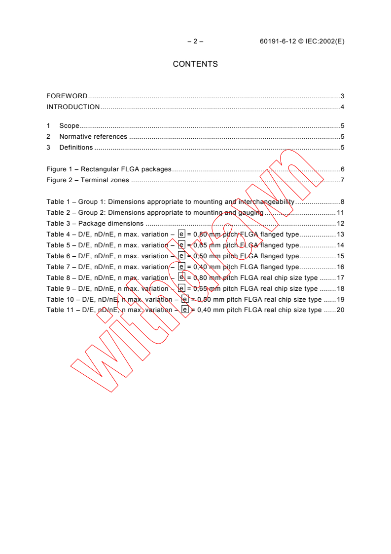
CONTENTS
FOREWORD.3
INTRODUCTION.4
1 Scope.5
2 Normative references .5
3 Definitions .5
Figure 1 – Rectangular FLGA packages.6
Figure 2 – Terminal zones .7
Table 1 – Group 1: Dimensions appropriate to mounting and interchangeability.8
Table 2 – Group 2: Dimensions appropriate to mounting and gauging.11
Table 3 – Package dimensions .12
e
Table 4 – D/E, nD/nE, n max. variation – = 0,80 mm pitch FLGA flanged type.13
Table 5 – D/E, nD/nE, n max. variation – e = 0,65 mm pitch FLGA flanged type.14
e
Table 6 – D/E, nD/nE, n max. variation – = 0,50 mm pitch FLGA flanged type.15
Table 7 – D/E, nD/nE, n max. variation – e = 0,40 mm pitch FLGA flanged type.16
e
Table 8 – D/E, nD/nE, n max. variation – = 0,80 mm pitch FLGA real chip size type .17
Table 9 – D/E, nD/nE, n max. variation – e = 0,65 mm pitch FLGA real chip size type .18
e
Table 10 – D/E, nD/nE, n max. variation – = 0,50 mm pitch FLGA real chip size type .19
e
Table 11 – D/E, nD/nE, n max. variation – = 0,40 mm pitch FLGA real chip size type .20
60191-6-12 © IEC:2002(E) – 3 –
INTERNATIONAL ELECTROTECHNICAL COMMISSION
___________
MECHANICAL STANDARDIZATION OF SEMICONDUCTOR DEVICES –
Part 6-12: General rules for the preparation of outline drawings
of surface mounted semiconductor device packages –
Design guide for fine-pitch land grid array (FLGA) –
Rectangular type
FOREWORD
1) The IEC (International Electrotechnical Commission) is a worldwide organization for standardization comprising
all national electrotechnical committees (IEC National Committees). The object of the IEC is to promote
international co-operation on all questions concerning standardization in the electrical and electronic fields. To
this end and in addition to other activities, the IEC publishes International Standards. Their preparation is
entrusted to technical committees; any IEC National Committee interested in the subject dealt with may
participate in this preparatory work. International, governmental and non-governmental organizations liaising
with the IEC also participate in this preparation. The IEC collaborates closely with the International
Organization for Standardization (ISO) in accordance with conditions determined by agreement between the
two organizations.
2) The formal decisions or agreements of the IEC on technical matters express, as nearly as possible, an
international consensus of opinion on the relevant subjects since each technical committee has representation
from all interested National Committees.
3) The documents produced have the form of recommendations for international use and are published in the form
of standards, technical specifications, technical reports or guides and they are accepted by the National
Committees in that sense.
4) In order to promote international unification, IEC National Committees undertake to apply IEC International
Standards transparently to the maximum extent possible in their national and regional standards. Any
divergence between the IEC Standard and the corresponding national or regional standard shall be clearly
indicated in the latter.
5) The IEC provides no marking procedure to indicate its approval and cannot be rendered responsible for any
equipment declared to be in conformity with one of its standards.
6) Attention is drawn to the possibility that some of the elements of this International Standard may be the subject
of patent rights. The IEC shall not be held responsible for identifying any or all such patent rights.
International Standard IEC 60191-6-12 has been prepared by subcommittee 47D: Mechanical
standardization of semiconductor devices, of IEC technical committee 47: Semiconductor
devices.
The text of this standard is based on the following documents:
FDIS Report on voting
47D/493/FDIS 47D/507/RVD
Full information on the voting for the approval of this standard can be found in the report on
voting indicated in the above table.
This publication has been drafted in accordance with the ISO/IEC Directives, Part 3.
A bilingual version of this publication may be issued at a later date.
The committee has decided that the contents of this publication will remain unchanged
until 2004. At this date, the publication will be
• reconfirmed;
• withdrawn;
• replaced by a revised edition, or
• amended.
– 4 – 60191-6-12 © IEC:2002(E)
INTRODUCTION
The demand for area array style packages exists because of the multi-functions and high
performance of electrical equipment. The objective of this design guide is to standardize
outlines and to get interchangeability of FLGA rectangular type packages. The terminal pitch
and package outlines of these fine-pitch array packages are smaller than those of LGA
packages.
60191-6-12 © IEC:2002(E) – 5 –
MECHANICAL STANDARDIZATION OF SEMICONDUCTOR DEVICES –
Part 6-12: General rules for the preparation of outline drawings
of surface mounted semiconductor device packages –
Design guide for fine-pitch land grid array (FLGA) –
Rectangular type
1 Scope
This part of IEC 60191 provides common outline drawings and dimensions for all types of
structures and composed materials of fine-pitch land grid array (hereinafter called FLGA)
whose terminal pitch is less than, or equal to, 0,80 mm and whose package body outline is
rectangular.
2 Normative references
The following referenced documents are indispensable for the application of this document.
For dated references, only the edition cited applies. For undated references, the latest edition
of the referenced document (including any amendments) applies.
IEC 60191 (all parts), Mechanical standardization of semiconductor devices
3 Definitions
For the purposes of this part of IEC 60191, the following definitions, as well as those given in
the other parts of this series, apply.
3.1
flanged type
type whose package body size (body length and width) consists of its own flange composed
around the encapsulation or lid
3.2
type of real chip size
type whose package body size (body length and width) consists of an encapsulation around
the real chip only
3.3
FLGA
packages with metal lands or metal bumps of which the terminal height is less than, or equal
to, 100 μm, and whose terminal pitch is less than, or equal to, 0,80 mm, positioned in an array
on the base plane of the package as external terminals
This package structure makes it possible to surface-mount the packages to the printed circuit board.
3.4
material designation
FLGA packages are classified according to the following two material designations:
3.4.1
plastic type (P-FLGA)
plastic-type classification is assigned to packages which consist of resin substrate as
interposer material (for example, glass-epoxy, poly-imid)
3.4.2
ceramic type (C-FLGA)
ceramic-type classification is assigned to packages which consist of ceramic substrate as
interposer material
– 6 – 60191-6-12 © IEC:2002(E)
E
w
SB
NOTE 2
NOTE 3
4 ×
v
NOTE 1
y
1 SSS
S
NOTE 7 y
S
eE
B
ZE
A A
1 2
NOTE 7
Even type
nD
B
A A
1 2
NOTE 7
A B
B B
1 3
NOTE 6
Odd type
B B
2 4
A A
1 2
B
B
12 3
nE NOTE 4
A A
3 4
∅b
∅X MSAB
SE
NOTE 5 IEC 1240/02
Figure 1 – Rectangular FLGA packages
SD
A
A BC
ZD
A
1 w SA
D
eD
A
60191-6-12 © IEC:2002(E) – 7 –
NOTE 1 Indicates seating plane. Seating plane is defined by the plane that the carrier contacts to the mount
surface.
NOTE 2 Indicates positional tolerance of the index mark.
NOTE 3 Bilateral tolerance zone is applied to four sides of the package body.
NOTE
...


Questions, Comments and Discussion
Ask us and Technical Secretary will try to provide an answer. You can facilitate discussion about the standard in here.
Loading comments...