CISPR TR 16-3:2003/AMD1:2005
(Amendment)Amendment 1 - Specification for radio disturbance and immunity measuring apparatus and methods - Part 3: CISPR technical reports
Amendment 1 - Specification for radio disturbance and immunity measuring apparatus and methods - Part 3: CISPR technical reports
In the present amendment to CISPR 16-3, experimental results show a relationship between the degradation in quality of digital communication systems and APD (amplitude probability distribution) characteristics of disturbance. These results show that APD measurement of disturbance is suitable for evaluating its interference potential on digital communication systems. Therefore APD measurement may be applicable to the compliance test of some products or product families, such as microwave ovens.
General Information
- Status
- Published
- Publication Date
- 10-Jul-2005
- Technical Committee
- CIS/A - Radio-interference measurements and statistical methods
- Current Stage
- DELPUB - Deleted Publication
- Start Date
- 10-Aug-2010
- Completion Date
- 13-Feb-2026
Relations
- Effective Date
- 05-Sep-2023
- Effective Date
- 05-Sep-2023
Overview
CISPR TR 16-3:2003/AMD1:2005 (Amendment 1) updates Part 3 of the CISPR 16 series by adding technical-report material that links amplitude probability distribution (APD) measurement of radiated disturbance to the real‑world performance degradation of digital communication systems. Based on experimental data (using actual microwave ovens and a noise simulator), the amendment shows APD is a suitable metric for evaluating interference potential and may be applicable for compliance testing of certain product families (for example, microwave ovens).
Key Topics
- APD characteristics of disturbance: introduction and empirical APD curves demonstrating how noise amplitude distributions relate to communication degradation.
- Measurement methodology: standardized test set‑ups using fully anechoic chambers, horn antennas, isolators and attenuators to inject and measure disturbance; APD measuring points defined in test configurations.
- Performance metrics: use of Bit Error Rate (BER) and throughput as the primary indicators of communication quality (examples include W‑CDMA, wireless LAN, Bluetooth and PHS).
- Noise normalisation and parameters: results presented relative to a noise power density N0, including average and RMS values derived from APD data; discussion of C/N (carrier-to-noise) relationships.
- Use of noise simulators vs. real sources: comparisons showing how a noise simulator can be adjusted to emulate transformer‑type and inverter‑type microwave oven emissions.
- Frequency and bandwidth considerations: APD and performance correlations demonstrated across representative RF channels used by WLAN, Bluetooth, W‑CDMA and PHS.
Applications
- EMC testing and compliance: supports incorporating APD measurement into conformity assessment procedures when evaluating interference risk from intermittent or pulsed radiated noise sources.
- Product families with impulsive or non‑Gaussian noise: particularly relevant for devices like microwave ovens and other household appliances that produce non‑steady emissions.
- Wireless system impact assessment: provides a practical method to predict how real‑world disturbance will affect wireless services (throughput/B ER) used in design verification and pre‑compliance testing.
- Test development and validation: helps test laboratories and manufacturers validate noise simulators and test set‑ups by comparing APD and system performance.
Who should use this standard
- EMC test engineers and laboratories
- Product designers and compliance officers (household appliances, consumer electronics)
- Wireless system integrators and RF test teams assessing interference susceptibility
- Regulators and standards developers updating EMC test methods
Related Standards
- CISPR 16 series (measuring apparatus and methods) - this amendment supplements CISPR TR 16‑3.
- IEC/CISPR publications on radiated disturbance and immunity testing.
Keywords: CISPR TR 16-3 Amendment 1, APD measurement, amplitude probability distribution, EMC testing, microwave oven interference, BER, wireless throughput, digital communication systems.
Get Certified
Connect with accredited certification bodies for this standard

TL 9000 QuEST Forum
Telecommunications quality management system.

ANCE
Mexican certification and testing association.

Intertek Slovenia
Intertek testing, inspection, and certification services in Slovenia.
Sponsored listings
Frequently Asked Questions
CISPR TR 16-3:2003/AMD1:2005 is a technical report published by the International Electrotechnical Commission (IEC). Its full title is "Amendment 1 - Specification for radio disturbance and immunity measuring apparatus and methods - Part 3: CISPR technical reports". This standard covers: In the present amendment to CISPR 16-3, experimental results show a relationship between the degradation in quality of digital communication systems and APD (amplitude probability distribution) characteristics of disturbance. These results show that APD measurement of disturbance is suitable for evaluating its interference potential on digital communication systems. Therefore APD measurement may be applicable to the compliance test of some products or product families, such as microwave ovens.
In the present amendment to CISPR 16-3, experimental results show a relationship between the degradation in quality of digital communication systems and APD (amplitude probability distribution) characteristics of disturbance. These results show that APD measurement of disturbance is suitable for evaluating its interference potential on digital communication systems. Therefore APD measurement may be applicable to the compliance test of some products or product families, such as microwave ovens.
CISPR TR 16-3:2003/AMD1:2005 is classified under the following ICS (International Classification for Standards) categories: 33.100.10 - Emission; 33.100.20 - Immunity. The ICS classification helps identify the subject area and facilitates finding related standards.
CISPR TR 16-3:2003/AMD1:2005 has the following relationships with other standards: It is inter standard links to CISPR TR 16-3:2003, CISPR TR 16-3:2010. Understanding these relationships helps ensure you are using the most current and applicable version of the standard.
CISPR TR 16-3:2003/AMD1:2005 is available in PDF format for immediate download after purchase. The document can be added to your cart and obtained through the secure checkout process. Digital delivery ensures instant access to the complete standard document.
Standards Content (Sample)
TECHNICAL
CISPR
REPORT
16-3
AMENDMENT 1
2005-07
INTERNATIONAL SPECIAL COMMITTEE ON RADIO INTERFERENCE
Amendment 1
Specification for radio disturbance and immunity
measuring apparatus and methods –
Part 3:
CISPR technical reports
IEC 2005 Droits de reproduction réservés Copyright - all rights reserved
International Electrotechnical Commission, 3, rue de Varembé, PO Box 131, CH-1211 Geneva 20, Switzerland
Telephone: +41 22 919 02 11 Telefax: +41 22 919 03 00 E-mail: inmail@iec.ch Web: www.iec.ch
PRICE CODE
Commission Electrotechnique Internationale S
International Electrotechnical Commission
МеждународнаяЭлектротехническаяКомиссия
For price, see current catalogue
– 2 – TR/CISPR 16-3 Amend. 1 IEC:2005(E)
FOREWORD
This amendment has been prepared by CISPR subcommittee A: Radio interference measure-
ments and statistical methods.
The text of this amendment is based on the following documents:
DTR Report on voting
CISPR/A/572/DTR CISPR/A/586/RVC
Full information on the voting for the approval of this amendment can be found in the report
on voting indicated in the above table.
The committee has decided that the contents of this amendment and the base publication will
remain unchanged until the maintenance result date indicated on the IEC web site under
"http://webstore.iec.ch" in the data related to the specific publication. At this date, the
publication will be
• reconfirmed,
• withdrawn,
• replaced by a revised edition, or
• amended.
Page 10
4 Technical reports
Add, on page 186, after the existing subclause 4.6, the following new subclause:
4.7 Correlation between amplitude probability distribution (APD) characteristics of
disturbance and performance of digital communication systems
4.7.1 Introduction
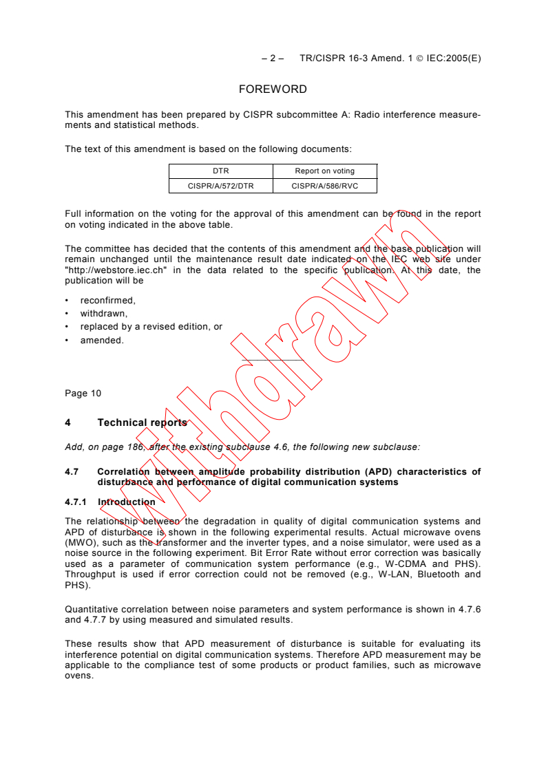
The relationship between the degradation in quality of digital communication systems and
APD of disturbance is shown in the following experimental results. Actual microwave ovens
(MWO), such as the transformer and the inverter types, and a noise simulator, were used as a
noise source in the following experiment. Bit Error Rate without error correction was basically
used as a parameter of communication system performance (e.g., W-CDMA and PHS).
Throughput is used if error correction could not be removed (e.g., W-LAN, Bluetooth and
PHS).
Quantitative correlation between noise parameters and system performance is shown in 4.7.6
and 4.7.7 by using measured and simulated results.
These results show that APD measurement of disturbance is suitable for evaluating its
interference potential on digital communication systems. Therefore APD measurement may be
applicable to the compliance test of some products or product families, such as microwave
ovens.
TR/CISPR 16-3 Amend. 1 IEC:2005(E) – 3 –
4.7.2 Influence on a wireless LAN system
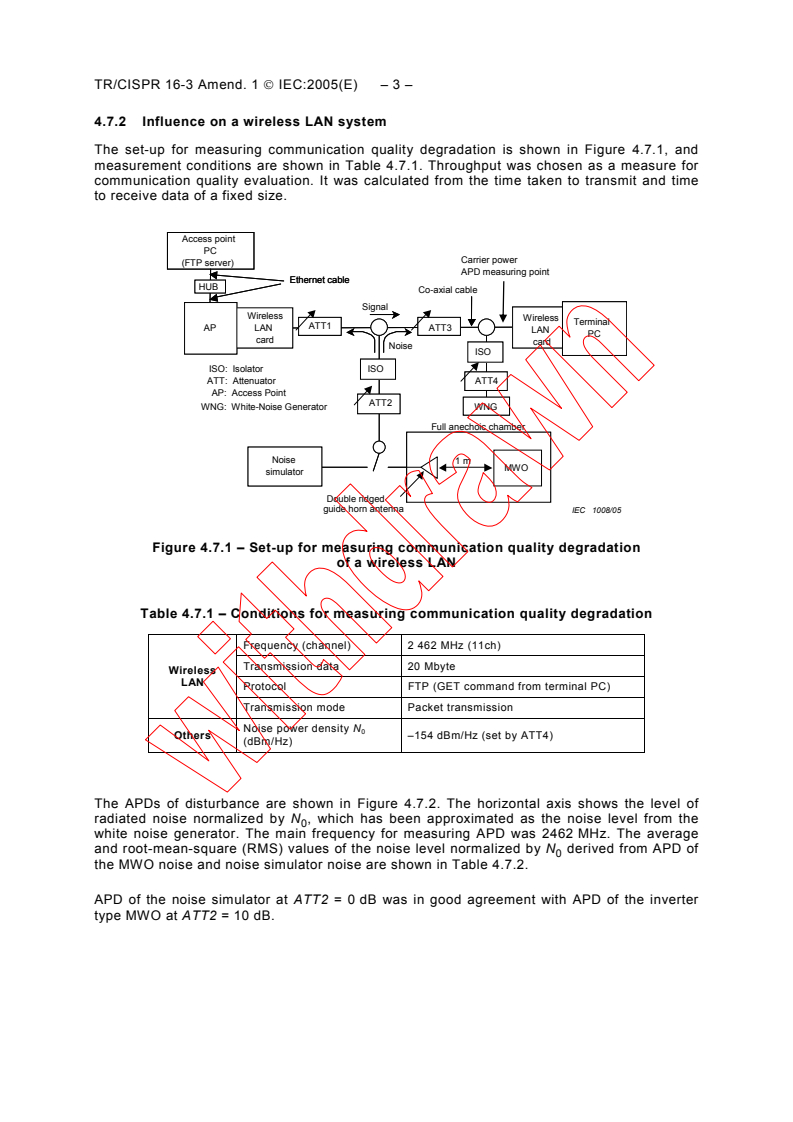
The set-up for measuring communication quality degradation is shown in Figure 4.7.1, and
measurement conditions are shown in Table 4.7.1. Throughput was chosen as a measure for
communication quality evaluation. It was calculated from the time taken to transmit and time
to receive data of a fixed size.
Access point
PC
Carrier power
(FTP server)
APD measuring point
EEttherhernenet cat cablblee
HUBHUB
Co-axial cable
Signal
Wireless
Wireless
TTeermrmiinalnal
ATT1
APAP LAN ATT3
LAN
PCPC
card
card
Noise
ISISOO
ISISOO
ISO: Isolator
ATT: Attenuator ATT4
AP: Access Point
ATT2
WNG: White-Noise Generator WNG
Full anechoic chamber
Noise
1 m
MWMWOO
simulator
1 m
Double ridged
guide horn antenna
IEC 1008/05
Figure 4.7.1 – Set-up for measuring communication quality degradation
of a wireless LAN
Table 4.7.1 – Conditions for measuring communication quality degradation
Frequency (channel) 2 462 MHz (11ch)
Transmission data 20 Mbyte
Wireless
LAN
Protocol FTP (GET command from terminal PC)
Transmission mode Packet transmission
Noise power density N
Others –154 dBm/Hz (set by ATT4)
(dBm/Hz)
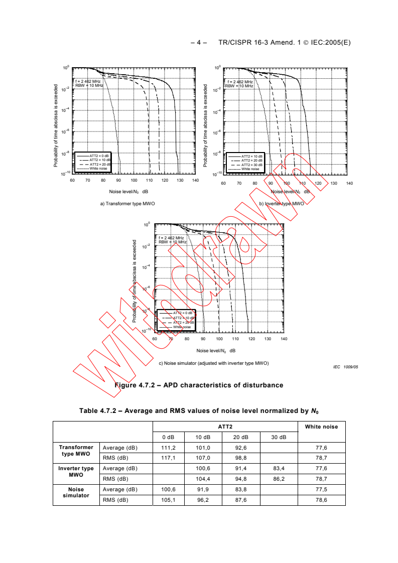
The APDs of disturbance are shown in Figure 4.7.2. The horizontal axis shows the level of
radiated noise normalized by N , which has been approximated as the noise level from the
white noise generator. The main frequency for measuring APD was 2462 MHz. The average
and root-mean-square (RMS) values of the noise level normalized by N derived from APD of
the MWO noise and noise simulator noise are shown in Table 4.7.2.
APD of the noise simulator at ATT2 = 0 dB was in good agreement with APD of the inverter
type MWO at ATT2 = 10 dB.
– 4 – TR/CISPR 16-3 Amend. 1 IEC:2005(E)
0 0
10 10
f = 2 462 MHz
f = 2 462 MHz
RBW = 10 MHz RBW = 10 MHz
–2
–2
–4
–4
–6
–6
–8 –8
10 10
ATT2 = 0 dB
ATT2 = 10 dB
ATT2 = 10 dB ATT2 = 20 dB
ATT2 = 20 dB
ATT2 = 30 dB
White noise
White noise
–10 –10
60 70 80 90 100 110 120 130 140
60 70 80 90 100 110 120 130 140
Noise level/N dB Noise level/N dB
0 0
a) Transformer type MWO b) Inverter type MWO
f = 2 462 MHz
RBW = 10 MHz
–2
–4
–6
–8
ATT2 = 0 dB
ATT2 = 10 dB
ATT2 = 20 dB
White noise
–10
60 70 80 90 100 110 120 130 140
Noise level/N0 dB
c) Noise simulator (adjusted with inverter type MWO)
IEC 1009/05
Figure 4.7.2 – APD characteristics of disturbance
Table 4.7.2 – Average and RMS values of noise level normalized by N
ATT2 White noise
0 dB 10 dB 20 dB 30 dB
Transformer
Average (dB) 111,2 101,0 92,6 77,6
type MWO
RMS (dB) 117,1 107,0 98,8 78,7
Inverter type Average (dB) 100,6 91,4 83,4 77,6
MWO
RMS (dB) 104,4 94,8 86,2 78,7
Noise Average (dB) 100,6 91,9 83,8 77,5
simulator
RMS (dB) 105,1 96,2 87,6 78,6
Probability of time abscissa is exceeded
Probability of time abscissa is exceeded
Probability of time abscissa is exceeded
TR/CISPR 16-3 Amend. 1 IEC:2005(E) – 5 –
The measured communication quality degradation for various amounts of attenuation of
injected noise is shown in Figure 4.7.3.
The horizontal axis shows C/N , where C is the sub-carrier power and N is the noise power
0 0
density.
600 600
500 500
ATT2 = 0 dB
ATT2 = 10 dB
ATT2 = 10 dB
ATT2 = 20 dB
ATT2 = 20 dB ATT2 =30 dB
White noise
White noise
60 70 80 90 100 110 120 130 140
60 70 80 90 100 110 120 130 140
C/N dB dB
0 C/N0
a) Transformer type MWO b) Inverter type MWO
ATT2 = 0 dB
100 ATT2 = 10 dB
ATT2 = 20 dB
White noise
60 70 80 90 100 110 120 130 140
C/N dB
c) Noise simulator (adjusted with inverter type MWO)
IEC 1010/05
Figure 4.7.3 – Wireless LAN throughput influenced by noise
The throughput influenced by a transformer type MWO is 400 kbytes/s or more when C/N is
90 dB or more, and decreases rapidly when C/N is below 90 dB. This tendency is almost the
same irrespective of the noise level. On the other hand, the throughput influenced by an
inverter type MWO decreases almost in proportion to the noise level. The throughput
influenced by a noise simulator has almost the same degradation characteristics as that for an
inverter type MWO.
4.7.3 Influence on a Bluetooth system
The setup for measuring communication quality degradation is shown in Figure 4.7.4, and
measurement conditions are shown in Table 4.7.3.
Throughput was chosen as the measure for communication quality evaluation.
Throughput kbyte/s
Throughput kbyte/s
Throughput kbyte/s
– 6 – TR/CISPR 16-3 Amend. 1 IEC:2005(E)
CCaarrirrier poer powweerr
APD mAPD meeaassuurriningg po poiinntt
Co-axial cable
Signal
Terminal
TTeermrmiinalnal P PCC
BBluetoluetooothth
Bluetooth
ATT1 ATT3
((FTFTPP s seervrveerr)) PC
card
card
(client)
Noise
ISISOO
ISO
ISO: Isolator
ATT4ATT4
ATT: Attenuator
WNG: White-noise generator ATT2
Fully anechoic
WNWNGG
chamber
Full anechoic chamber
NoNoiseise
1 m
MWMWOO
simsimuulatolatorr
1 m
Double ridged
guide horn antenna
IEC 1011/05
Figure 4.7.4 – Set-up for measuring the communication quality degradation of Bluetooth
Table 4.7.3 – Conditions for measuring communication quality degradation of Bluetooth
Frequency 2 400 – 2 483,5 MHz
Transmission data 2,5 Mbyte
Bluetooth
Protocol FTP (GET command from terminal PC)
Transmission mode Packet exchange data transmission mode
Noise power density N
Others -148 dBm/Hz (set by ATT4)
(dBm/Hz)
The APDs at a frequency of 2 441 MHz are shown in Fig. 4.7.5, and the average and RMS
values of noise level normalized by N are shown in Table 4.7.4.
0 0
10 10
f = 2 441 MHz f = 2 441 MHz
RBW = 1 MHz RBW = 1 MHz
–2 –2
10 10
–4 –4
10 10
–6 –6
10 10
ATT2 = 0 dB ATT2 = 0 dB
–8 –8
10 10
ATT2 = 10 dB ATT2 = 10 dB
ATT2 = 20 dB
ATT2 = 20 dB
White noise
White noise
–10 –10
10 10
40 50 60 70 80 90 100 110 120 40 50 60 70 80 90 100 110 120
Noise level/N dB Noise level/N dB
0 0
a) Transformer type MWO b) Inverter type MWO
IEC 1012/05
Figure 4.7.5 – APD of disturbance of actual MWO (2 441MHz)
Probability of time abscissa is exceeded
Probability of time abscissa is exceeded
TR/CISPR 16-3 Amend. 1 IEC:2005(E) – 7 –
Table 4.7.4 – Average and RMS values of noise level normalized by N
ATT2 White noise
0 dB 10 dB 20 dB 30 dB
Transformer type Average (dB) 89,8 80,8 73,7 67,1
MWO
RMS (dB) 99,2 90,2 82,5 68,3
Inverter type Average (dB) 70,7 65,4 63,5 67,1
MWO RMS (dB) 80,6 73,3 66,0 68,3
The APDs measured at 2 460 MHz, where the noise level of an MWO is at maximum, are
shown in Figure 4.7.6, and the average and RMS values of noise normalized by N are shown
in Table 4.7.5. The noise level is about 10 dB larger than that at the frequency of 2 441 MHz.
The APD of the noise simulator at ATT2 = 0 dB is in good agreement with that of the inverter
type MWO at ATT2 = 10 dB.
0 0
10 10
f = 2 460 MHz f = 2 460 MHz
RBW = 1 MHz
RBW = 1 MHz
–2 –2
10 10
–4 –4
10 10
–6 –6
10 10
–8 –8 ATT2 = 0 dB
ATT2 = 0 dB
10 10
ATT2 = 10 dB
ATT2 = 10 dB
ATT2 = 20 dB
ATT2 = 20 dB
White noise
White noise
–10 –10
10 10
40 50 60 70 80 90 100 110 120 40 50 60 70 80 90 100 110 120
Noise level/N dB Noise level/N dB
0 0
a) Transformer type MWO b) Inverter type MWO
f = 2 460 MHz
RBW = 1 MHz
–2
–4
–6
–8
ATT2 = 0 dB
ATT2 = 10 dB
White noise
–10
40 50 60 70 80 90 100 110 120
Noise level/N dB
c) Noise simulator (adjusted with inverter MWO)
IEC 1013/05
Figure 4.7.6 – APD characteristics of disturbance (2 460 MHz)
Probability of time abscissa is exceeded
Probability of time abscissa is exceeded
Probability of time abscissa is exceeded
– 8 – TR/CISPR 16-3 Amend. 1 IEC:2005(E)
Table 4.7.5 – Average and RMS values of noise level normalized by N
ATT2 White noise
0 dB 10 dB 20 dB 30 dB
Transformer Average (dB) 87,8 78,4 71,4 67,1
type MWO
RMS (dB) 94,9 85,4 78,0 68,3
Inverter type Average (dB) 70,7 65,4 63,5 67,1
MWO
RMS (dB) 80,6 73,3 66,0 68,3
Noise Average (dB) 77,6 69,8 67,1
simulator
RMS (dB) 84,1 75,5 68,3
The measured communication quality degradation for various amounts of attenuation of
injected noise is shown in Figure 4.7.7.
There is only a minor difference in degradation caused by the level of noise between a
transformer and an inverter type MWO. This is because Bluetooth performs frequency
hopping, and is hard to be influenced by noise continuously. Furthermore, there is almost no
difference in communication quality degradation for a noise simulator.
70 70
60 60
50 50
40 40
30 30
20 20
ATT2 = 0 dB
ATT2 = 0 dB
ATT2 = 10 dB
ATT2 = 10 dB
10 10
ATT2 = 20 dB
ATT2 = 20 dB
White noise
White noise
0 0
60 55 50 45 40 35 30 25 60 55 50 45 40 35 30 25
ATT1 dB ATT1 dB
a) Transformer type MWO b) Inverter type MWO
ATT2 = 0 dB
ATT2 = 10 dB
White noise
60 55 50 45 40 35 30 25
ATT1 dB
c) Noise simulator (adjusted with inverter type MWO)
IEC 1014/05
Figure 4.7.7 – Throughput of Bluetooth influenced by noise
Throughput kbyte/s
Throughput kbyte/s
Throughput kbyte/s
TR/CISPR 16-3 Amend. 1 IEC:2005(E) – 9 –
According to the specifications, Bluetooth controls the transmission power automatically
depending on the communication situation. The sub-carrier power at the reception point
cannot be obtained uniquely since transmission power may change when ATT1 is changed.
The horizontal axis in this figure shows the attenuation of signal power.
4.7.4 Influence on a W-CDMA system
The set-up for measuring communication quality degradation is shown in Figure 4.7.8, and
measurement conditions are shown in Table 4.7.6.
Bit error rate (BER) was chosen as the measure for communication quality evaluation.
Base station simulator
Data
BER
BER
measuring
equipment
Decode
Encode Path
ReReveverrssee
search
diffusion
Diffusion
Signal
ReRececeivivee
Transmit
Signal
ATT
W-CDMA
terminal
・
ATT1
ATT3
Carrier power
APD measuring point
ISO
ISO: Isolator
ATT: Attenuator
ATT2
AMP: Amplifier
AMP
Fully anechoic chamber
Noise
1 m
simulator MWMWOO
1 m
Double ridged
guide horn antenna IEC 1015/05
Figure 4.7.8 – Setup for measuring the BER of W-CDMA
Table 4.7.6 – Conditions for measuring communication quality degradation of W-CDMA
Frequency 2 137,6 MHz (downlink)
Chip rate 3,84 Mcps
Spread rate Uplink: DPDCH 64 / downlink: DPCH 128
Base band
Data rate 12,2 kbps (acoustic)
simulator
Transmission data 6 Mbit
RMC communication test (UE turn)
Transmission mode
3GPP TS34.121
The measured APDs of the noise are shown in Figure 4.7.9, and the average and RMS values
of the noise level normalized by N are shown in Table 4.7.7. The APD of the noise simulator
at ATT2 = 0 dB is in good agreement with the APD of the inverter type MWO at ATT2 = 10 dB.
– 10 – TR/CISPR 16-3 Amend. 1 IEC:2005(E)
f = 2 137,6 MHz
f = 2 137,6 MHz
RBW = 5 MHz
–2
RBW = 5 MHz
–2
–4
–4
–6
–6
–8
–8
ATT2 = 0 dB
ATT2 = 0 dB
ATT2 = 10 dB
ATT2 = 10 dB
–10
–10
40 50 60 70 80 90 100 110 120
40 50 60 70 80 90 100 110 120
Noise level/N dB Noise level/N dB
0 0
a) Transformer type MWO
b) Inverter type MWO
f = 2 137,6 MHz
RBW = 5 MHz
–2
–4
–6
–8
ATT2 = 10 dB
ATT2 = 20 dB
ATT2 = 30 dB
–10
40 50 60 70 80 90 100 110 120
Noise level/N dB
c) Noise simulator (adjusted with inverter MWO)
IEC 1016/05
Figure 4.7.9 – APD characteristics of disturbance
Table 4.7.7 – Average and RMS values of noise level normalized by N
ATT2 Receiver noise
0 dB 10 dB 20 dB 30 dB
Transformer Average (dB) 71,1 67,7 67,2
type MWO
RMS (dB) 75,1 69,4 68,6
Inverter type Average (dB) 71,6 68,0 67,2
MWO
RMS (dB) 74,7 69,4 68,6
Noise Average (dB) 77,1 70,4 67,7 67,2
simulator
RMS (dB) 83,3 74,7 69,3 68,6
The measured communication quality degradation for various amounts of attenuation of
injected noise is shown in Figure 4.7.10.
Probability of time abscissa is exceeded
Probability of time abscissa is exceeded
Probability of time abscissa is exceeded
TR/CISPR 16-3 Amend. 1 IEC:2005(E) – 11 –
For both types of MWO, the BER was degraded by several dB after a 10 dB change in noise
level. Moreover, BER characteristics influenced by the noise simulator are in good agreement
in these measurement results.
–1 –1
10 10
–2 –2
10 10
–3 –3
10 10
–4 –4
10 10
–5 –5
10 10
ATT2 = 0 dB
–6 –6
10 ATT2 = 0 dB 10
ATT2 = 10 dB
ATT2 =10 dB
Without noise
Without noise
–7 –7
10 10
40 45 50 55 60 65 40 45 50 55 60 65
C/N dB C/N dB
0 0
a) Transformer type MWO b) Inverter type MWO
–1
–2
–3
–4
–5
ATT2 = 10 dB
ATT2 = 20 dB
–6 ATT2 = 30 dB
Without noise
–7
40 45 50 55 60 65
C/N dB
c) Noise simulator (adjusted with inverter MWO)
IEC 1017/05
Figure 4.7.10 – BER of W-CDMA caused by radiation noise
4.7.5 Influence on Personal Handy Phone System (PHS)
The set-ups for measuring communication quality degradation are shown in Figures 4.7.11
and 4.7.12, and conditions for measuring throughput and BER are shown in Tables 4.7.8 and
4.7.9.
Throughput and BER were chosen as measures for evaluating the communication quality of
PHS.
The measured APDs are shown in Figure 4.7.13, and the average and RMS values of noise
normalized by N are shown in Table 4.7.10.
BER
BER
BER
– 12 – TR/CISPR 16-3 Amend. 1 IEC:2005(E)
Carrier power
ISDISDNN
APD measuring point
sisimmuullaatotorr
Co-axial cable
Signal
RReecceeiviviningg
PHS
TransmTransmiittttiingng
TA
ATT1 ATT3
PCPC
card
PCPC
Noise
ISO
Serial cable ISO
ISO: Isolator ATT4
ATT2
ATT: Attenuator
WNG: White-noise generator
Fully anechoic
WNG
AMP
TA: Terminal adapter chamber
1 m
NoiNoisse e
MWO
MWO
1 m
sisimmuullaatotorr
Double ridged
guide horn antenna
IEC 1018/05
Figure 4.7.11 – Set-up for measuring the PHS throughput
Signal
Carrier power
Block
APD measuring point
Co-axial cable
Signal
Terminal
SSiignalgnal
PHS
ATT3
ATT1
PC
generatgeneratoror
card
Noise
IS Test mode
ISO: Isolator
ISO
ATT: Attenuator ATT4
WNG: White-noise generator
ATT2
Fully anechoic
WNG
chamber
Noise
1 m
MWMWOO
simulator
1 m
Double ridged
guide horn antenna
IEC 1019/05
Figure 4.7.
...


Questions, Comments and Discussion
Ask us and Technical Secretary will try to provide an answer. You can facilitate discussion about the standard in here.
Loading comments...