Surface chemical analysis — Determination of surface elemental contamination on silicon wafers by total-reflection X-ray fluorescence (TXRF) spectroscopy

ISO 14706:2014 specifies a TXRF method for the measurement of the atomic surface density of elemental contamination on chemomechanically polished or epitaxial silicon wafer surfaces. The method is applicable to the following: elements of atomic number from 16 (S) to 92 (U); contamination elements with atomic surface densities from 1 × 10¹⁰ atoms/cm2 to 1 × 10¹⁴ atoms/cm2; contamination elements with atomic surface densities from 5 × 10⁸ atoms/cm2 to 5 × 10¹² atoms/cm2 using a VPD (vapour-phase decomposition) specimen preparation method.

Analyse chimique des surfaces — Détermination de la contamination en éléments à la surface des tranches de silicium par spectroscopie de fluorescence X à réflexion totale

General Information

Status
Published
Publication Date
24-Jul-2014
Current Stage
9093 - International Standard confirmed
Completion Date
17-Jun-2021
Ref Project

Relations

Buy Standard

Standard
ISO 14706:2014 - Surface chemical analysis -- Determination of surface elemental contamination on silicon wafers by total-reflection X-ray fluorescence (TXRF) spectroscopy
English language
25 pages
sale 15% off
Preview
sale 15% off
Preview

Standards Content (Sample)

INTERNATIONAL ISO
STANDARD 14706
Second edition
2014-08-01
Surface chemical analysis —
Determination of surface elemental
contamination on silicon wafers by
total-reflection X-ray fluorescence
(TXRF) spectroscopy
Analyse chimique des surfaces — Détermination de la contamination
en éléments à la surface des tranches de silicium par spectroscopie de
fluorescence X à réflexion totale
Reference number
ISO 14706:2014(E)
©
ISO 2014

---------------------- Page: 1 ----------------------
ISO 14706:2014(E)

COPYRIGHT PROTECTED DOCUMENT
© ISO 2014
All rights reserved. Unless otherwise specified, no part of this publication may be reproduced or utilized otherwise in any form
or by any means, electronic or mechanical, including photocopying, or posting on the internet or an intranet, without prior
written permission. Permission can be requested from either ISO at the address below or ISO’s member body in the country of
the requester.
ISO copyright office
Case postale 56 • CH-1211 Geneva 20
Tel. + 41 22 749 01 11
Fax + 41 22 749 09 47
E-mail copyright@iso.org
Web www.iso.org
Published in Switzerland
ii © ISO 2014 – All rights reserved

---------------------- Page: 2 ----------------------
ISO 14706:2014(E)

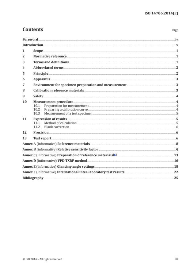
Contents Page
Foreword .iv
Introduction .v
1 Scope . 1
2 Normative reference . 1
3 Terms and definitions . 1
4 Abbreviated terms . 2
5 Principle . 2
6 Apparatus . 3
7 Environment for specimen preparation and measurement . 3
8 Calibration reference materials . 3
9 Safety . 4
10 Measurement procedure . 4
10.1 Preparation for measurement . 4
10.2 Preparing a calibration curve . 4
10.3 Measurement of a test specimen . 5
11 Expression of results . 5
11.1 Method of calculation . 5
11.2 Blank correction . 6
12 Precision . 6
13 Test report . 6
Annex A (informative) Reference materials . 8
Annex B (informative) Relative sensitivity factor . 9
[6]
Annex C (informative) Preparation of reference materials .13
Annex D (informative) VPD-TXRF method .16
Annex E (informative) Glancing-angle settings .18
Annex F (informative) International inter-laboratory test results .22
Bibliography .25
© ISO 2014 – All rights reserved iii

---------------------- Page: 3 ----------------------
ISO 14706:2014(E)

Foreword
ISO (the International Organization for Standardization) is a worldwide federation of national standards
bodies (ISO member bodies). The work of preparing International Standards is normally carried out
through ISO technical committees. Each member body interested in a subject for which a technical
committee has been established has the right to be represented on that committee. International
organizations, governmental and non-governmental, in liaison with ISO, also take part in the work.
ISO collaborates closely with the International Electrotechnical Commission (IEC) on all matters of
electrotechnical standardization.
The procedures used to develop this document and those intended for its further maintenance are
described in the ISO/IEC Directives, Part 1. In particular the different approval criteria needed for the
different types of ISO documents should be noted. This document was drafted in accordance with the
editorial rules of the ISO/IEC Directives, Part 2 (see www.iso.org/directives).
Attention is drawn to the possibility that some of the elements of this document may be the subject of
patent rights. ISO shall not be held responsible for identifying any or all such patent rights. Details of
any patent rights identified during the development of the document will be in the Introduction and/or
on the ISO list of patent declarations received (see www.iso.org/patents).
Any trade name used in this document is information given for the convenience of users and does not
constitute an endorsement.
For an explanation on the meaning of ISO specific terms and expressions related to conformity
assessment, as well as information about ISO’s adherence to the WTO principles in the Technical Barriers
to Trade (TBT) see the following URL: Foreword - Supplementary information
The committee responsible for this document is ISO/TC 201, Surface chemical analysis.
This second edition cancels and replaces the first edition (ISO 14706:2000), which has been technically
revised.
iv © ISO 2014 – All rights reserved

---------------------- Page: 4 ----------------------
ISO 14706:2014(E)

Introduction
This International Standard was prepared for the measurement of surface elemental contamination
on silicon wafers on the basis of three existing standards: ASTM F 1526, SEMI Standard M33, and a
UCS (Ultra-Clean Society) standard published by the Institute of Basic Semiconductor Technology
Development.
TXRF needs reference materials to perform quantitative analyses. Certified reference materials are not
10 2
available at low densities of 10 atoms/cm . Even if they were available, the possibility of contamination
from the environment reduces the shelf life of such reference materials.
Therefore, the TXRF reference materials are to be prepared and analysed for calibration by each relevant
analytical laboratory. Thus, two standards, one for the TXRF measurement procedure and the other for
the preparation of reference materials, are necessary. This International Standard concerns the former
part.
© ISO 2014 – All rights reserved v

---------------------- Page: 5 ----------------------
INTERNATIONAL STANDARD ISO 14706:2014(E)
Surface chemical analysis — Determination of surface
elemental contamination on silicon wafers by total-
reflection X-ray fluorescence (TXRF) spectroscopy
1 Scope
This International Standard specifies a TXRF method for the measurement of the atomic surface density
of elemental contamination on chemomechanically polished or epitaxial silicon wafer surfaces.
The method is applicable to the following:
— elements of atomic number from 16 (S) to 92 (U);
10 2 14
— contamination elements with atomic surface densities from 1 × 10 atoms/cm to 1 × 10
2
atoms/cm ;
8 2 12 2
— contamination elements with atomic surface densities from 5 × 10 atoms/cm to 5 × 10 atoms/cm
using a VPD (vapour-phase decomposition) specimen preparation method (see 3.4).
2 Normative reference
The following documents, in whole or in part, are normatively referenced in this document and are
indispensable for its application. For dated references, only the edition cited applies. For undated
references, the latest edition of the referenced document (including any amendments) applies.
ISO 14644-1, Cleanrooms and associated controlled environments — Part 1: Classification of air cleanliness
3 Terms and definitions
For the purposes of this document, the following terms and definitions apply.
3.1
total reflection
complete reflection of glancing X-ray radiation into a medium having larger X-ray optical density value
at a boundary between two media
Note 1 to entry: The refractive index of silicon for X-rays is less than 1. X-rays which are incident on the surface
at a small glancing angle are therefore, totally reflected from the surface at an angle equal to the glancing angle.
3.2
glancing angle
angle between the specimen surface plane and the virtual plane containing incident X-rays which
impinge on the sample surface
3.3
critical angle
glancing angle corresponding to the first point of inflection in the plot of the sample matrix X-ray
fluorescence against the glancing angle
© ISO 2014 – All rights reserved 1

---------------------- Page: 6 ----------------------
ISO 14706:2014(E)

3.4
VPD-TXRF method
method in which impurities on the surface are collected by the so-called VPD procedure, i.e. the non-
volatile products formed by acid decomposition of the oxide at the wafer surface are collected by a
droplet of collecting agent, usually ultra-pure hydrofluoric acid, and dried in a manner which gives the
least environmental contamination, the residue from the droplet, subsequently being analysed by TXRF
3.5
spurious peaks
detected peaks that do not originate from impurities on the silicon wafer
Note 1 to entry: Spurious peaks are due to fluorescent X-rays originating from elements in the detector or the X-ray
path. The fluorescent X-rays are excited by direct scattering or reflection of incident X-rays. This phenomenon
leads to an increase in the measurement error. Spurious peaks seriously affect analytical measurements in the
10 2 11 2
contamination range from ca. 10 atoms/cm to ca. 10 atoms/cm .
4 Abbreviated terms
FWHM full width at half maximum
RM reference material
SSD solid-state detector
SDD silicon drift detector
TXRF total-reflection X-ray fluorescence
VPD vapour-phase decomposition
5 Principle
When a specimen is irradiated with X-rays, fluorescence X-rays at characteristic energies of the elements
that constitute the specimen are generated. The intensities of the fluorescence X-rays are proportional
to the amounts of each element in the specimen.
Total reflection of the incident X-rays on the specimen reduces a penetration depth of the incident X-rays
in the specimen. This allows more selective excitation of the fluorescence X-rays from the surface region,
including atoms deposited on the surface of the silicon wafer. Consequently, a spectrum of fluorescence
X-rays with a large ratio of signal to background (S/B) and signal to noise (S/N) can be obtained.
The detection limit depends upon the atomic number, the excitation energy, the photon flux, the
detector resolution and energy-dependent detection efficiency, the energy bandwidth of the excitation
X-rays, the specimen-related shape and statistics of TXRF spectral background, the instrument-related
noise magnitude, the integration time, and the accuracy of calibration of the RM and the blank value.
For constant instrumental parameters, the interference-free detection limits vary over two orders of
magnitude as a function of the atomic number of the analyte element.
NOTE The depth of measurement can vary with the glancing angle, but in the case of film-type contamination
it is usually less than 5 nm. The area of measurement consists of a circle of ca. 10 mm in diameter, though it
varies depending on the relative position of the X-ray detector and the specimen. In the case of particulate-type
contamination on a clean surface, the yield of fluorescence X-rays varies depending on the sizes, distribution, and
constituent elements of the particles.
2 © ISO 2014 – All rights reserved

---------------------- Page: 7 ----------------------
ISO 14706:2014(E)

6 Apparatus
6.1 The apparatus for TXRF shall include at least the following components: an X-ray source; a
monochromator; a specimen stage capable of movement in three orthogonal directions; an X-ray detector
(SSD or SDD); and a computerized signal-processing system.
6.2 X-rays which have been monochromatized shall be used as the incident X-rays.
6.3 The fluorescence X-ray detector shall have sufficient energy resolution to analyse the Mn-K-L
II,III
line with an FWHM of 200 eV or less.
6.4 The specimen stage, which sets the glancing angle, shall be controlled to a reproducibility within
±0,17 mrad (0,01°) in the range between 0 mrad (0°) and 8,7 mrad (0,5°).
6.5 The atmosphere in the specimen chamber shall be able to be brought to a reduced pressure or
replaced with helium gas or nitrogen gas, as required.
7 Environment for specimen preparation and measurement
7.1 The local environment (i.e. airborne particles, temperature, humidity) for specimen preparation
and measurement shall be equal to or better than ISO Class 4 in accordance with ISO 14644-1.
NOTE The unwanted deposition of airborne particles which are composed of the elements that are being
measured will cause an increase in the error of measurement.
7.2 The mechanical vibration at the location where the apparatus is installed shall be as small as
–3 2
possible and shall not be greater than 5 × 10 m/s (0,5 Gal).
NOTE The mechanical vibration will degrade the energy resolution of the detection system, which will, in
turn, degrade the detection limits and peak deconvolution.
8 Calibration reference materials
8.1 Calibration reference materials (RMs) used to establish a reliable calibration procedure shall consist
of an RM on which known amounts of impurities have been deposited and a blank RM used to determine
the level of contamination of the calibration RM (see Annex A).
8.2 The RMs shall be prepared from a chemomechanically polished wafer with a certain quantity of Ni
or Fe uniformly deposited on its surface as the RM element. The atomic surface density of the RM element
12 2 13 2
shall be ca. 1 × 10 atoms/cm to 1 × 10 atoms/cm (see Annex C).
8.3 How the RM element is located on the RM surface shall be verified by an anglescan (see Annex E).
8.4 The amount of RM element deposited on the surface of the wafer shall be determined by a reliable
quantitative method of analysis.
8.5 The blank RM shall be a chemomechanically polished or epitaxial wafer. The magnitude of
contamination of the surface region of the blank RM shall be below the detection limit for specified
elements. The crystallographic orientation of the blank RM shall be the same as that of the RM.
8.6 The RM and the blank RM shall be stored in the same container.
© ISO 2014 – All rights reserved 3

---------------------- Page: 8 ----------------------
ISO 14706:2014(E)

9 Safety
This test method uses X-ray radiation. Consequently, it is absolutely essential to avoid exposing any part
of the body to the X-rays produced by the apparatus. It is especially important to keep hands and fingers
out of the path of the X-rays and to protect the eyes from scattered secondary X-ray radiation. Each
country has its own safety regulations and requirements concerning X-rays. These shall be observed.
10 Measurement procedure
10.1 Preparation for measurement
10.1.1 All specimens shall be chemomechanically polished or epitaxial wafers.
10.1.2 For the VPD-TXRF method, the impurities on the surface are collected by VPD, i.e. acid decomposition
in a droplet which is then dried in a manner that produces the least environmental contamination (see
Annex D).
10.1.3 For a series of measurements, including the calibration measurements, the crystal orientation of
the specimen on the specimen stage shall be the same for each specimen.
10.1.4 Set the glancing angle at between 25 % and 75 % of the critical angle.
NOTE 1 Due to the physical form of particulate-type contamination, an angle that is too low will cause a larger
error.
NOTE 2 The critical angle is a function of the incident X-ray energy. It is 3,20 mrad (0,18°) for 9,67 keV (W-L
II-
), 1,78 mrad (0,10°) for 17,44 keV (Mo-K-L ) and 2,72 mrad (0,16°) for 11,4 keV (Au-L ).
MIV II,III II-MIV
10.1.5 Set the following parameters as specified.
a) For a rotating anode, the excitation voltage of the X-ray source shall be 30 kV or more, with the
excitation current set to 200 mA or more and the integration time set to 500 s or more.
b) For a sealed Mo or W anode X-ray tube, the excitation voltage of the X-ray source shall be 30 kV or
more, with the excitation current set to 40 mA or more and the integration time set to 500 s or more.
c) If the X-ray intensity at the detector is too high for the detection system, the excitation current shall
be adjusted to a lower value to give an appropriate count rate.
10.1.6 Move the centre of the specimen under the centre of the detector. While rotating the specimen,
generate and measure fluorescence X-rays to find the azimuth with the least spurious peaks. When
possible, the measurement hereafter shall be conducted at the same azimuth.
If the apparatus does not allow the best-fit azimuth to be set at off-centre positions so as to avoid spurious
peaks, care shall be taken when evaluating the surface-mapping data.
10.2 Preparing a calibration curve
10.2.1 Measure the blank RM and determine the integrated intensity of the fluorescence X-rays generated
by the blank RM.
10.2.2 Measure the RM under the same conditions as specified in 10.2.1. In the case of the VPD-TXRF
method, place the residue from the RM under the centre of the detector.
4 © ISO 2014 – All rights reserved

---------------------- Page: 9 ----------------------
ISO 14706:2014(E)

10.2.3 Verify that the measured value of the integrated intensity of the X-rays generated by the blank RM
is less than 10 % of the integrated intensity from the RM.
If the integrated intensity from the blank RM is 10 % or more of that from the RM, discard both the RM
and the blank RM and prepare a new set comprising an RM and blank RM.
Carry out this check at appropriate intervals.
10.2.4 Determine the integrated intensity of the X-rays generated by the RM element by means of
procedure a) and/or b) specified below.
a) Smooth the measured numerical values by digital processing.
Determine the integrated intensity of the X-rays by subtracting the background from the measured
numerical values.
b) Determine the Gaussian function that best fits the measured numerical values. Then determine the
integrated intensity from the peak height and the half-width of the Gaussian function.
10.2.5 Obtain a calibration curve (a plot of the atomic surface density versus the integrated X-ray
intensity from the RM element). The curve shall pass through the origin.
10.3 Measurement of a test specimen
10.3.1 Measure the test specimen under the same conditions as specified in 10.1. If using the VPD-TXRF
method, place the residue from the test specimen under the centre of the detector.
10.3.2 Determine the integrated intensity of the X-rays generated by contamination elements in the
same manner as specified in 10.2.
When two or more fluorescence X-ray lines overlap, use the method of deconvolution to obtain the
integrated intensity of the X-rays for the subject element.
NOTE 1 The repeatability and reproducibility of the measurement for the subject element will vary with the
kind of X-ray used.
NOTE 2 Deviation of the glancing angle of the incident X-rays from the set value will increase the measurement
error.
NOTE 3 Greater surface roughness will increase the measurement error.
NOTE 4 The values obtained from VPD residues will depend greatly on the physical form of the residue and the
elements contained in the residue.
11 Expression of results
11.1 Method of calculation
By using Formulae (1) and (2), calculate the atomic surface density, C for each of the contamination
m
elements from the results obtained in Clause 10.
C
S
K= (1)
I
S
© ISO 2014 – All rights reserved 5

---------------------- Page: 10 ----------------------
ISO 14706:2014(E)

I
m
CK=× (2)
m
S
R
where
K is the slope of the calibration curve obtained in 10.2.5;
2
C is the atomic surface density of the RM element, in atoms/cm ;
S
I is the integrated intensity of the fluorescence X-rays from the RM element, in counts per sec-
S
ond (cps);
C is the atomic surface density of the contamination element on the test specimen, in atoms/
m
2
cm ;
I is the integrated intensity of the fluorescence X-rays from the contamination element on the
m
test specimen, in cps;
S is the relative sensitivity factor, which corrects for the difference in sensitivity for each ele-
R
ment.
NOTE In order to determine values of the relative sensitivity factor, S for other elements, measurements are
R
often made on two or more specimens with differing contents of these elements. The results can then be used to
prepare calibration curves other than those obtained using theoretical relative sensitivity factors. The relative
sensitivity factor can be determined in terms of these curves using the RM element or can be calculated as shown
in Annex B.
11.2 Blank correction
11 2
For measurements below 10 atoms/cm , where the instrumental blank is not negligible, the
atomic surface density, C shall be corrected by subtracting the atomic surface density, C of a fresh
m 0
contamination-free specimen, with the same crystal orientation, measured under the same conditions
as specified in 10.1 and 10.2 and calculated as described in 11.1.
12 Precision
An international inter-laboratory test programme based on the method specified in this International
Standard was carried out by 15 laboratories from Japan, Europe, and USA. Four test specimens and
one RM were distributed as one set. 17 sets of measurements were obtained from the 15 laboratories.
[1]
Repeatability and reproducibility were calculated in accordance with the principles of ISO 5725-2. A
statistical report of the inter-laboratory test is given in Annex F.
13 Test report
The test report shall include the following items:
a) specimen identification;
b) the kind(s) of X-ray source used, e.g. rotating-anode W-tube;
c) the excitation X-rays used, e.g. W-L -M ;
II IV
d) the voltage applied to the X-ray source, e.g. 30 kV;
e) the current applied to the X-ray source, e.g. 200 mA;
f) the glancing angle used, e.g. 1,8 mrad (0,10°);
g) the integration time, e.g. 500 s;
6 © ISO 2014 – All rights reserved

---------------------- Page: 11 ----------------------
ISO 14706:2014(E)

h) the method used to prepare the RM, e.g. SC1 dip method (see Annex A);
12 2
i) the atomic surface density of the RM element (Ni or Fe), e.g. Ni 1,05 × 10 atoms/cm ;
j) the measurement location on the test specimen, e.g. centre of wafer;
k) the calibration method used, i.e. procedure a) or b) in 10.2.4;
l) the name(s) of the element(s) on the test specimen and the atomic surface density of each.
© ISO 2014 – All rights reserved 7

---------------------- Page: 12 ----------------------
ISO 14706:2014(E)

Annex A
(informative)

Reference materials
A.1 Reference materials for this International Standard can be prepared by the SC1 dip method
[which uses standard cleaning solution 1 (a silicon wafer cleaning solution consisting of water, ammonia,
12
and hydrogen peroxide)] or by the spin-coating method to give a surface Ni or Fe content of ca. 10
2 13 2
atoms/cm to 1 × 10 atoms/cm (see Annex C).
A.2 The Fe RM prepared by the SC1 dip method is preferred when the apparatus is installed in a
higher-class cleanroom.
A.3 The Ni RM is more commonly used for routine measurements.
A.4 One or more RMs should be prepared from each lot or batch.
A.5 Specimens from the same lot or batch are assumed to have the same atomic surface density.
A.6 The calibration of RMs is discussed in Annex C.
A.7 In the case of VPD-TXRF measurement, an RM consisting of a microdroplet residue containing
known amounts of impurities and deposited on a hydrophobic polished or epitaxial wafer can be used.
A.8 The VPD collection efficiency is assumed to be approximately 100 %.
8 © ISO 2014 – All rights reserved

---------------------- Page: 13 ----------------------
ISO 14706:2014(E)

Annex B
(informative)

Relative sensitivity factor
B.1 The relative sensitivity factor can be calculated from the model shown in Figure B.1.
Key
t measurement depth
Ω solid angle
Figure B.1 — Schematic illustration of TXRF
© ISO 2014 – All rights reserved 9

---------------------- Page: 14 ----------------------
ISO 14706:2014(E)

The X-ray intensity ΔI of measured spectrum L of element A, generated from the very thin layer Δt is
L
given by:
w (μ//)ρ
A AP,λ
 
Δ=II exp(− μρ/) ρφttcos(ec μρ/) ρφΔ cosec ×
Lp0,λλ{}Mp,,Mpλ
 
(/μρ)
Mp,λ
(B.1)
γ −1
δΩ
A
 
ωμg exp(− /)ρρtcosecψ
{ }}
AL ML,λ
 
γ 4π
A
where
I is the incident X-ray intensity at wavelength λ ;
0,λP P
[2]
(μ/ρ) is the mass absorption coefficient for the X-rays incident on specimen M;
M,λP
ρ is the density of specimen M;
w is the mass fraction of element A in the specimen;
A
(μ/ρ) is the mass absorption coefficient for the X-rays incident on element A;
A,λP
[2]
γ is the jump ratio of the series shell of element A at the absorption edge;
A
[2][3][4]
ω is the fluorescence yield of the series shell of element A;
A
[5]
g is the relative transition probability of the measured spectrum L;
L
(μ/ρ) is the mass absorption coefficient of measured spectrum L at wavelength λ for speci-
M,λL L
men M.
Assuming that the value of the depth t is very small:
 
exp(− μρ/) ρφtcosec =1
{}
M,λp
 

 
exp(− μρ/) ρψtcosec =1
{}
M,λL
 
Adding double excitation of total reflection, Formula (B.1) can be expressed as follows:
γ −1 δΩ
A
II= 2 wt(/μρ)cωρg osecϕ (B.2)
Lp0,λλAA, p AL
γ 4π
A
As the value of the depth t is very small:
wrtC= A N (B.3)
()
AA r,AA
where
C is the atomic surface density of element A;
A
A is the atomic mass of element A;
r,A
N is Avogadro’s number.
A
10 © ISO 2014 – All rights reserved

---------------------- Page: 15 ----------------------
ISO 14706:2014(E)

From Formulae (B.2) and (B.3):
I γ −1
δΩ
L A
S ==2IA(/Ne)cos c(φμ/)ρ ω g
A 0,λλpr,AA A, p AL
C 4π γ
A A
The relative sensitivity factor, S is thus given by:
R
γ −1
A
(/μρ) ω g ⋅⋅AE
Ap,,λ AL rA A
S γ
A A
S == (B.4)
R
γ −1
S
RM
RM
(/μρ) ω g ⋅⋅AE
RM,λp RM λλRM rR, MRM
γ
RM
where
A is the relative atomic mass of the RM element;
r,RM
E , E are the attenuation factors in the solid-state detector for wavelengths λ and λ , respec-
A RM L RM
tively.
The above formula is based on the assumption that the specimen has a uniform density and a smooth
surface, that monochromatized X-rays with no divergency are used, and that no multiple scattering or
excitation by o
...

Questions, Comments and Discussion

Ask us and Technical Secretary will try to provide an answer. You can facilitate discussion about the standard in here.