ISO 19214:2024
(Main)Microbeam analysis — Analytical electron microscopy — Method of determination for apparent growth direction of nanocrystals by transmission electron microscopy
Microbeam analysis — Analytical electron microscopy — Method of determination for apparent growth direction of nanocrystals by transmission electron microscopy
This document gives a method for determination of the apparent growth direction of nanocrystals by transmission electron microscopy. This method is applicable to all kinds of wire-like crystalline materials synthetized by various methods. This document can also guide in determining an axis direction of the second-phase particles in steels, alloys, or other materials. The applicable diameter or width of the crystals to be tested is in the range of tens to one hundred nanometres, depending on the accelerating voltage of the transmission electron microscope (TEM) and the material itself. Position, which is curved, twisted, and folded, to determine the apparent growth direction, should not be used.
Titre manque
General Information
Relations
Standards Content (Sample)
International
Standard
ISO 19214
Second edition
Microbeam analysis — Analytical
2024-10
electron microscopy — Method
of determination for apparent
growth direction of nanocrystals by
transmission electron microscopy
Reference number
© ISO 2024
All rights reserved. Unless otherwise specified, or required in the context of its implementation, no part of this publication may
be reproduced or utilized otherwise in any form or by any means, electronic or mechanical, including photocopying, or posting on
the internet or an intranet, without prior written permission. Permission can be requested from either ISO at the address below
or ISO’s member body in the country of the requester.
ISO copyright office
CP 401 • Ch. de Blandonnet 8
CH-1214 Vernier, Geneva
Phone: +41 22 749 01 11
Email: copyright@iso.org
Website: www.iso.org
Published in Switzerland
ii
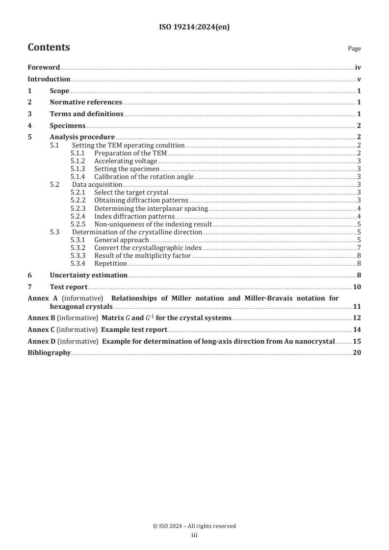
Contents Page
Foreword .iv
Introduction .v
1 Scope . 1
2 Normative references . 1
3 Terms and definitions . 1
4 Specimens. 2
5 Analysis procedure . 2
5.1 Setting the TEM operating condition .2
5.1.1 Preparation of the TEM .2
5.1.2 Accelerating voltage .3
5.1.3 Setting the specimen .3
5.1.4 Calibration of the rotation angle .3
5.2 Data acquisition .3
5.2.1 Select the target crystal .3
5.2.2 Obtaining diffraction patterns .3
5.2.3 Determining the interplanar spacing .4
5.2.4 Index diffraction patterns.4
5.2.5 Non-uniqueness of the indexing result .5
5.3 Determination of the crystalline direction .5
5.3.1 General approach .5
5.3.2 Convert the crystallographic index .7
5.3.3 Result of the multiplicity factor .8
5.3.4 Repetition .8
6 Uncertainty estimation . 8
7 Test report .10
Annex A (informative) Relationships of Miller notation and Miller-Bravais notation for
hexagonal crystals .11
-1
Annex B (informative) Matrix G and G for the crystal systems .12
Annex C (informative) Example test report . 14
Annex D (informative) Example for determination of long-axis direction from Au nanocrystal .15
Bibliography .20
iii
Foreword
ISO (the International Organization for Standardization) is a worldwide federation of national standards
bodies (ISO member bodies). The work of preparing International Standards is normally carried out through
ISO technical committees. Each member body interested in a subject for which a technical committee
has been established has the right to be represented on that committee. International organizations,
governmental and non-governmental, in liaison with ISO, also take part in the work. ISO collaborates closely
with the International Electrotechnical Commission (IEC) on all matters of electrotechnical standardization.
The procedures used to develop this document and those intended for its further maintenance are described
in the ISO/IEC Directives, Part 1. In particular, the different approval criteria needed for the different types
of ISO document should be noted. This document was drafted in accordance with the editorial rules of the
ISO/IEC Directives, Part 2 (see www.iso.org/directives).
ISO draws attention to the possibility that the implementation of this document may involve the use of (a)
patent(s). ISO takes no position concerning the evidence, validity or applicability of any claimed patent
rights in respect thereof. As of the date of publication of this document, ISO had not received notice of (a)
patent(s) which may be required to implement this document. However, implementers are cautioned that
this may not represent the latest information, which may be obtained from the patent database available at
www.iso.org/patents. ISO shall not be held responsible for identifying any or all such patent rights.
Any trade name used in this document is information given for the convenience of users and does not
constitute an endorsement.
For an explanation of the voluntary nature of standards, the meaning of ISO specific terms and expressions
related to conformity assessment, as well as information about ISO's adherence to the World Trade
Organization (WTO) principles in the Technical Barriers to Trade (TBT), see www.iso.org/iso/foreword.html.
This document was prepared by Technical Committee ISO/TC 202, Microbeam analysis, Subcommittee SC 3,
Analytical electron microscopy.
This second edition cancels and replaces the first edition (ISO 19214:2017), which has been technically
revised.
The main changes are as follows:
— the title, introduction and scope have been revised;
— Clause 3 has been revised;
— Figures 1 and 2 have been replaced;
— Annex D has been added;
— editorial revisions have been made.
Any feedback or questions on this document should be directed to the user’s national standards body. A
complete listing of these bodies can be found at www.iso.org/members.html.
iv
Introduction
Nanocrystals are a main component in some advanced materials, especially nanomaterials, and also
appear in traditional materials, such as needle-shaped precipitates in steels and alloys. Controlling the
microstructure of these materials during fabrication is very important for quality control considerations.
To control the microstructure and thereby improve the service properties of the relevant materials, the
apparent growth direction, or the longest axis of the nanocrystals is one of the essential parameters. This
direction of nanocrystals is generally determined by transmission electron microscopy (TEM).
v
International Standard ISO 19214:2024(en)
Microbeam analysis — Analytical electron microscopy —
Method of determination for apparent growth direction of
nanocrystals by transmission electron microscopy
1 Scope
This document gives a method for determination of the apparent growth direction of nanocrystals by
transmission electron microscopy. This method is applicable to all kinds of wire-like crystalline materials
synthetized by various methods. This document can also guide in determining an axis direction of the
second-phase particles in steels, alloys, or other materials. The applicable diameter or width of the crystals
to be tested is in the range of tens to one hundred nanometres, depending on the accelerating voltage of
the transmission electron microscope (TEM) and the material itself. Position, which is curved, twisted, and
folded, to determine the apparent growth direction, should not be used.
2 Normative references
The following documents are referred to in the text in such a way that some or all of their content constitutes
the requirements of this document. For dated references, only the edition cited applies. For undated
references, the latest edition of the referenced document (including any amendments) applies.
ISO 15932, Microbeam analysis — Analytical electron microscopy — Vocabulary
ISO 25498:2018, Microbeam analysis — Analytical electron microscopy — Selected area electron diffraction
analysis using a transmission electron microscope
3 Terms and definitions
For the purposes of this document, the terms and definitions given in ISO 15932 and the following apply.
ISO and IEC maintain terminology databases for use in standardization at the following addresses:
— ISO Online browsing platform: available at https:// www .iso .org/ obp
— IEC Electropedia: available at https:// www .electropedia .org/
3.1
nanocrystal
discrete piece of crystalline material exhibiting a dimensional anisotropy with an axial elongation in one of
the three nanocrystalline lattice direction in the nanoscale
3.2
apparent growth direction
crystalline direction which is parallel to the longest dimension of a single crystal
Note 1 to entry: Apparent growth direction does not involve mechanisms of the phase interface migration.
3.3
Miller notation
indexing system for diffraction patterns, which describes a crystal lattice by three axes coordinate
3.4
Miller-Bravais notation
indexing system for diffraction patterns of hexagonal crystal, which describes the lattice by four axes
coordinate
3.5
reciprocal vector
g
hkl
coordinate vector of hkl lattice point in the reciprocal lattice
Note 1 to entry: Reciprocal vector g is perpendicular to the plane (hkl) of crystal, its length is inversely proportional
hkl
to the interplanar spacing d .
hkl
[SOURCE: ISO 25498:2018, 3.8, modified — Note 1 to entry has been modified. ]
3.6
R vector
R
hkl
coordinate vector from the central spot 000 to the diffraction spot hkl in a diffraction pattern
[SOURCE: ISO 25498:2018, 3.9, modified — Note 1 to entry has been removed.]
3.7
reciprocal space
imaginary space where planes of atoms are represented by reciprocal points and all lengths are the inverse
of their length in real space
4 Specimens
4.1 The sample crystals shall be clean, without contamination or oxidation. They are stable under electron
beam irradiation during TEM analysis.
4.2 Powder or extracted powder specimens of the crystals may be analysed. The sample powder shall be
well dispersed by a suitable technique so that individual crystals can be observed under the TEM.
NOTE One of the techniques in common use is ultrasonic dispersion. In this method, the sample powder is
immersed in ethanol or pure water and dispersed by ultrasonication for about 0,5 h to 1 h, then dropped onto the
supporting film surface of a microgrid. Then, the microgrids are dried at room temperature. The wire-like crystals
are usually parallel to
...


Questions, Comments and Discussion
Ask us and Technical Secretary will try to provide an answer. You can facilitate discussion about the standard in here.