ISO 20263:2024
(Main)Microbeam analysis — Analytical electron microscopy — Method for the determination of interface position in the cross-sectional image of the layered materials
Microbeam analysis — Analytical electron microscopy — Method for the determination of interface position in the cross-sectional image of the layered materials
This document specifies a procedure for the determination of the averaged interface position between two different layered materials recorded in the cross-sectional image of the multi-layered material. This document does not apply for determining the simulated interface of the multi-layered materials expected through the multi-slice simulation (MSS) method. This document is applicable to the cross-sectional images of multi-layered materials recorded using a transmission electron microscope (TEM) or a scanning transmission electron microscope (STEM) and cross-sectional elemental mapping images using an energy dispersive X-ray spectrometer (EDS) or an electron energy loss spectrometer (EELS). This document is also applicable to digitized images recorded on an image sensor built into a digital camera, a digital memory set in the PC or an imaging plate, where the digitalized image is obtained by converting an analogue image recorded on photographic film using an image scanner.
Analyse par microfaisceaux — Microscopie électronique analytique — Méthode de détermination de la position d'interface dans l'image de coupe transversale des matériaux en couches
General Information
Relations
Standards Content (Sample)
International
Standard
ISO 20263
Second edition
Microbeam analysis — Analytical
2024-11
electron microscopy — Method
for the determination of interface
position in the cross-sectional
image of the layered materials
Analyse par microfaisceaux — Microscopie électronique
analytique — Méthode de détermination de la position
d'interface dans l'image de coupe transversale des matériaux en
couches
Reference number
© ISO 2024
All rights reserved. Unless otherwise specified, or required in the context of its implementation, no part of this publication may
be reproduced or utilized otherwise in any form or by any means, electronic or mechanical, including photocopying, or posting on
the internet or an intranet, without prior written permission. Permission can be requested from either ISO at the address below
or ISO’s member body in the country of the requester.
ISO copyright office
CP 401 • Ch. de Blandonnet 8
CH-1214 Vernier, Geneva
Phone: +41 22 749 01 11
Email: copyright@iso.org
Website: www.iso.org
Published in Switzerland
ii
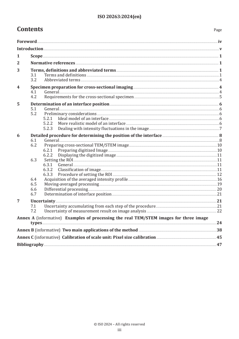
Contents Page
Foreword .iv
Introduction .v
1 Scope . 1
2 Normative references . 1
3 Terms, definitions and abbreviated terms . 1
3.1 Terms and definitions .1
3.2 Abbreviated terms .4
4 Specimen preparation for cross-sectional imaging . 4
4.1 General .4
4.2 Requirements for the cross-sectional specimen .5
5 Determination of an interface position . 6
5.1 General .6
5.2 Preliminary considerations .6
5.2.1 Ideal model of an interface .6
5.2.2 More realistic model of an interface .6
5.2.3 Dealing with intensity fluctuations in the image .7
6 Detailed procedure for determining the position of the interface . 8
6.1 General .8
6.2 Preparing cross-sectional TEM/STEM image .10
6.2.1 Preparing digitized Image .10
6.2.2 Displaying the digitized image .11
6.3 Setting the ROI .11
6.3.1 General .11
6.3.2 Classification of image.11
6.3.3 Procedure of setting the ROI . 12
6.4 Acquisition of the averaged intensity profile .16
6.5 Moving-averaged processing .19
6.6 Differential processing . 20
6.7 Determination of interface position .21
7 Uncertainty .21
7.1 Uncertainty accumulating from each step of the procedure.21
7.2 Uncertainty of measurement result on image analysis . 22
Annex A (informative) Examples of processing the real TEM/STEM images for three image
types .24
Annex B (informative) Two main applications of the method .38
Annex C (informative) Calibration of scale unit: Pixel size calibration .45
Bibliography . 47
iii
Foreword
ISO (the International Organization for Standardization) is a worldwide federation of national standards
bodies (ISO member bodies). The work of preparing International Standards is normally carried out through
ISO technical committees. Each member body interested in a subject for which a technical committee
has been established has the right to be represented on that committee. International organizations,
governmental and non-governmental, in liaison with ISO, also take part in the work. ISO collaborates closely
with the International Electrotechnical Commission (IEC) on all matters of electrotechnical standardization.
The procedures used to develop this document and those intended for its further maintenance are described
in the ISO/IEC Directives, Part 1. In particular, the different approval criteria needed for the different types
of ISO document should be noted. This document was drafted in accordance with the editorial rules of the
ISO/IEC Directives, Part 2 (see www.iso.org/directives).
ISO draws attention to the possibility that the implementation of this document may involve the use of (a)
patent(s). ISO takes no position concerning the evidence, validity or applicability of any claimed patent
rights in respect thereof. As of the date of publication of this document, ISO had not received notice of (a)
patent(s) which may be required to implement this document. However, implementers are cautioned that
this may not represent the latest information, which may be obtained from the patent database available at
www.iso.org/patents. ISO shall not be held responsible for identifying any or all such patent rights.
Any trade name used in this document is information given for the convenience of users and does not
constitute an endorsement.
For an explanation of the voluntary nature of standards, the meaning of ISO specific terms and expressions
related to conformity assessment, as well as information about ISO's adherence to the World Trade
Organization (WTO) principles in the Technical Barriers to Trade (TBT), see www.iso.org/iso/foreword.html.
This document was prepared by Technical Committee ISO/TC 202, Microbeam analysis, Subcommittee SC 3,
Analytical electron microscopy.
This second edition cancels and replaces the first edition (ISO 20263:2017), which has been technically
revised.
The main changes are as follows:
— introduction has been revised;
— terms and sources in Clause 3 have been revised;
— subclauses 5.2.2, 5.2.3, 6.1, 6.2.1, 6.7, 7.1, 7.2, A.4.1, B.2.3 and B.2.4 have been revised;
— figures have been revised.
Any feedback or questions on this document should be directed to the user’s national standards body. A
complete listing of these bodies can be found at www.iso.org/members.html.
iv
Introduction
Multi-layered materials are widely used in the production of semiconductor devices, various kinds of sensors,
coating films for optical element, new functional materials, etc. One of the factors used to determine the
characteristics of multi-layered materials is the layer thickness, for evaluation of products and verification
of the production process. In practice, measuring the total thickness and/or the thickness of each layer
and checking the uniformity of thickness and/or flatness of the interface are often done using recorded
images of the materials. Evaluations can be made from the cross-sectional TEM/STEM images by accurately
determining the averaged interface position between two different layered materials.
In relation to the determination of the interface position in the HR atomic imaging, analysis by the multi-
slice simulation (MSS) method can be applied for the target measurement, if the atomic structural models
can be constructed. However, in real materials, there are a lot of cases when they cannot, such as:
— the interface between amorphous layers, or layers of amorphous substance and crystal;
— the interface recorded in low-resolution image in which the atomic columns cannot be identified:
— for very thick single-layered material;
— for thick multi-layered material.
This document gives the method to determine the averaged interface position using a differential processing
of the accumulated intensity profile obtained from the ROI set in the cross-sectional TEM/STEM image of
the multi-layered material. The thickness of the layer that can be applied ranges from a few nanometers to a
few micrometers. Thus, this document is not intended for the determination of the simulated position of the
layer interface analysed by the MSS method.
v
International Standard ISO 20263:2024(en)
Microbeam analysis — Analytical electron microscopy —
Method for the determination of interface position in the
cross-sectional image of the layered materials
1 Scope
This document specifies a procedure for the determination of the averaged interface position between
two different layered materials recorded in the cross-sectional image of the multi-layered material. This
document does not apply for determining the simulated interface of the multi-layered materials expected
through the multi-slice simulation (MSS) method.
This document is applicable to the cross-sectional images of multi-layered materials recorded using a
transmission electron microscope (TEM) or a scanning transmission electron microscope (STEM) and cross-
sectional elemental mapping images using an energy dispersive X-ray spectrometer (EDS) or an electron
energy loss spectrometer (EELS). This document is also applicable to digitized images recorded on an image
sensor built into a digital camera, a digital memory set in the PC or an imaging plate, where the digitalized
image is obtained by converting an analogue image recorded on photographic film using an image scanner.
2 Normative references
There are no normative references in this document.
3 Terms, definitions and abbreviated terms
3.1 Terms and definitions
For the purposes of this document, the following terms and definitions apply.
ISO and IEC maintain terminology databases for use in standardization at the following addresses:
— ISO Online browsing platform: available at https:// www .iso .org/ obp
— IEC Electropedia
...


Questions, Comments and Discussion
Ask us and Technical Secretary will try to provide an answer. You can facilitate discussion about the standard in here.