ASTM E983-05
(Guide)Standard Guide for Minimizing Unwanted Electron Beam Effects in Auger Electron Spectroscopy
Standard Guide for Minimizing Unwanted Electron Beam Effects in Auger Electron Spectroscopy
SCOPE
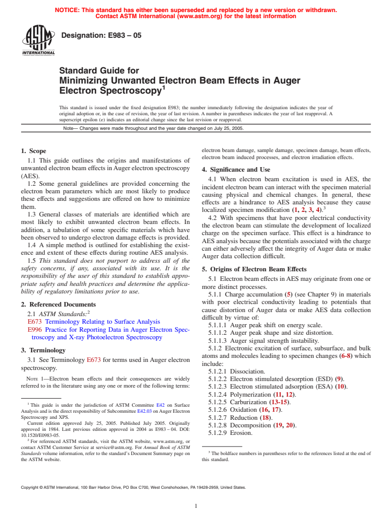
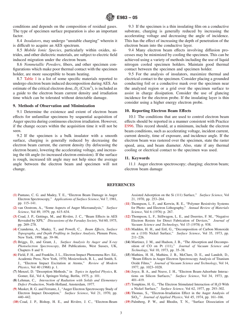
1.1 This guide outlines the origins and manifestations of unwanted electron beam effects in Auger electron spectroscopy (AES).
1.2 Some general guidelines are provided concerning the electron beam parameters which are most likely to produce these effects and suggestions are offered on how to minimize them.
1.3 General classes of materials are identified which are most likely to exhibit unwanted electron beam effects. In addition, a tabulation of some specific materials which have been observed to undergo electron damage effects is provided.
1.4 A simple method is outlined for establishing the existence and extent of these effects during routine AES analysis.
1.5 This standard does not purport to address all of the safety concerns, if any, associated with its use. It is the responsibility of the user of this standard to establish appropriate safety and health practices and determine the applicability of regulatory limitations prior to use.
General Information
Relations
Standards Content (Sample)
NOTICE: This standard has either been superseded and replaced by a new version or withdrawn.
Contact ASTM International (www.astm.org) for the latest information
Designation:E983–05
Standard Guide for
Minimizing Unwanted Electron Beam Effects in Auger
1
Electron Spectroscopy
This standard is issued under the fixed designation E983; the number immediately following the designation indicates the year of
original adoption or, in the case of revision, the year of last revision. A number in parentheses indicates the year of last reapproval. A
superscript epsilon (´) indicates an editorial change since the last revision or reapproval.
Note— Changes were made throughout and the year date changed on July 25, 2005.
electron beam damage, sample damage, specimen damage, beam effects,
1. Scope
electron beam induced processes, and electron irradiation effects.
1.1 This guide outlines the origins and manifestations of
unwantedelectronbeam effects inAuger electron spectroscopy
4. Significance and Use
(AES).
4.1 When electron beam excitation is used in AES, the
1.2 Some general guidelines are provided concerning the
incident electron beam can interact with the specimen material
electron beam parameters which are most likely to produce
causing physical and chemical changes. In general, these
these effects and suggestions are offered on how to minimize
effects are a hindrance to AES analysis because they cause
them.
3
localized specimen modification (1, 2, 3, 4).
1.3 General classes of materials are identified which are
4.2 With specimens that have poor electrical conductivity
most likely to exhibit unwanted electron beam effects. In
the electron beam can stimulate the development of localized
addition, a tabulation of some specific materials which have
charge on the specimen surface. This effect is a hindrance to
been observed to undergo electron damage effects is provided.
AES analysis because the potentials associated with the charge
1.4 A simple method is outlined for establishing the exist-
can either adversely affect the integrity of Auger data or make
ence and extent of these effects during routine AES analysis.
Auger data collection difficult.
1.5 This standard does not purport to address all of the
safety concerns, if any, associated with its use. It is the
5. Origins of Electron Beam Effects
responsibility of the user of this standard to establish appro-
5.1 Electron beam effects inAES may originate from one or
priate safety and health practices and determine the applica-
more distinct processes.
bility of regulatory limitations prior to use.
5.1.1 Charge accumulation (5) (see Chapter 9) in materials
with poor electrical conductivity leading to potentials that
2. Referenced Documents
cause distortion of Auger data or make AES data collection
2
2.1 ASTM Standards:
difficult by virtue of:
E673 Terminology Relating to Surface Analysis
5.1.1.1 Auger peak shift on energy scale.
E996 Practice for Reporting Data in Auger Electron Spec-
5.1.1.2 Auger peak shape and size distortion.
troscopy and X-ray Photoelectron Spectroscopy
5.1.1.3 Auger signal strength instability.
5.1.2 Electronic excitation of surface, subsurface, and bulk
3. Terminology
atoms and molecules leading to specimen changes (6-8) which
3.1 See Terminology E673 for terms used inAuger electron
include:
spectroscopy.
5.1.2.1 Dissociation.
NOTE 1—Electron beam effects and their consequences are widely
5.1.2.2 Electron stimulated desorption (ESD) (9).
referred to in the literature using any one or more of the following terms:
5.1.2.3 Electron stimulated adsorption (ESA) (10).
5.1.2.4 Polymerization (11, 12).
5.1.2.5 Carburization (13-15).
1
This guide is under the jurisdiction of ASTM Committee E42 on Surface
5.1.2.6 Oxidation (16, 17).
Analysis and is the direct responsibility of Subcommittee E42.03 onAuger Electron
Spectroscopy and XPS.
5.1.2.7 Reduction (18).
Current edition approved July 25, 2005. Published July 2005. Originally
5.1.2.8 Decomposition (19, 20).
approved in 1984. Last previous edition approved in 2004 as E983 – 04. DOI:
5.1.2.9 Erosion.
10.1520/E0983-05.
2
For referenced ASTM standards, visit the ASTM website, www.astm.org, or
contact ASTM Customer Service at service@astm.org. For Annual Book of ASTM
3
Standards volume information, refer to the standard’s Document Summary page on The boldface numbers in parentheses refer to the references listed at the end of
the ASTM website. this standard.
Copyright © ASTM International, 100 Barr Harbor Drive, PO Box C700, West Conshohocken, PA 19428-2959, United States.
1
---------------------- Page: 1 ----------------------
E983–05
2
5.1.2.10 Diffusion. terms are being changed. A dose of C/cm is equivalent to
4 2 2 2
5.1.3 Charge accumulation in materials of poor electrical 10 C/m , while 1mA/cm is equivalent to 10A/m .
conductivity leading to specimen changes which include (21, 7.1.2 Specimenmaterialmodificationcanoftenberelatedto
22, 5) (see Chapter 8): the electron dose (D); that is, the number of elect
...


Questions, Comments and Discussion
Ask us and Technical Secretary will try to provide an answer. You can facilitate discussion about the standard in here.