ASTM E431-96(2002)
(Guide)Standard Guide to Interpretation of Radiographs of Semiconductors and Related Devices
Standard Guide to Interpretation of Radiographs of Semiconductors and Related Devices
SCOPE
1.1 This guide provides illustrations of radiographs of semiconductors and related devices. Low powered transistors (through the TO-11 case configuration), diodes, low-power rectifiers, power devices, and integrated circuits are illustrated with common assembly features. Particular areas of construction are featured for these devices detailing critical points of design or assembly.
1.2 This standard does not purport to address all of the safety concerns, if any, associated with its use. It is the responsibility of the user of this standard to establish appropriate safety and health practices and determine the applicability of regulatory limitations prior to use.
General Information
Relations
Standards Content (Sample)
NOTICE: This standard has either been superseded and replaced by a new version or withdrawn.
Contact ASTM International (www.astm.org) for the latest information
Designation: E 431 – 96 (Reapproved 2002)
Standard Guide to
Interpretation of Radiographs of Semiconductors and
Related Devices
This standard is issued under the fixed designation E 431; the number immediately following the designation indicates the year of
original adoption or, in the case of revision, the year of last revision. A number in parentheses indicates the year of last reapproval. A
superscript epsilon (e) indicates an editorial change since the last revision or reapproval.
1. Scope resulting from x-ray examinations (see Table 1) to ascertain
quality of assembly and workmanship.
1.1 This guide provides illustrations of radiographs of
4.2 Required attributes of the design features or other
semiconductors and related devices. Low powered transistors
construction details are not provided but are to be established
(through the TO-11 case configuration), diodes, low-power
as mutually agreed upon by manufacturers and users of these
rectifiers, power devices, and integrated circuits are illustrated
devices. Many devices share common assembly features; thus,
with common assembly features. Particular areas of construc-
these interpretations can be used for components not illus-
tion are featured for these devices detailing critical points of
trated.
design or assembly.
1.2 This standard does not purport to address all of the
5. Use of Illustrations
safety concerns, if any, associated with its use. It is the
5.1 The illustrations in this guide are for use in interpreting
responsibility of the user of this standard to establish appro-
radiographs of semiconductors and related devices. They
priate safety and health practices and determine the applica-
provide reference points and information on the critical areas
bility of regulatory limitations prior to use.
of such devices. These points must be clearly resolved in the
2. Referenced Documents radiographs being interpreted. The radiographs to be inter-
preted must comply with the requirements of Practice E 801 to
2.1 ASTM Standards:
ensure suitable image quality with minimal distortion. Addi-
E 801 Practice for Controlling Quality of Radiological Ex-
tional information on the application of radiographic tech-
amination of Electronic Devices
niques to semiconductors and electronic components may be
E 1161 Test Method for Radiologic Examination of Semi-
found in Test Method E 1161.
conductors and Electronic Components
5.2 The illustrations in this guide may also be used to
E 1255 Practice for Radioscopy
2 interpret the radioscopic images of semiconductors and related
E 1316 Terminology for Nondestructive Examinations
devices when using radioscopic techniques. The radioscopic
3. Terminology images to be interpreted must comply with the requirements of
Practice E 801 to ensure suitable image quality with minimal
3.1 Definitions of terms used in these reference illustrations
distortion. Additional information on the application of radio-
may be found in Terminology E 1316, Section D.
scopic techniques may be found in Test Method E 1161 and
4. Significance and Use
Practice E 1255.
4.1 Illustrations provided in this guide are intended for use
6. Description
as references to aid in interpreting film or nonfilm images
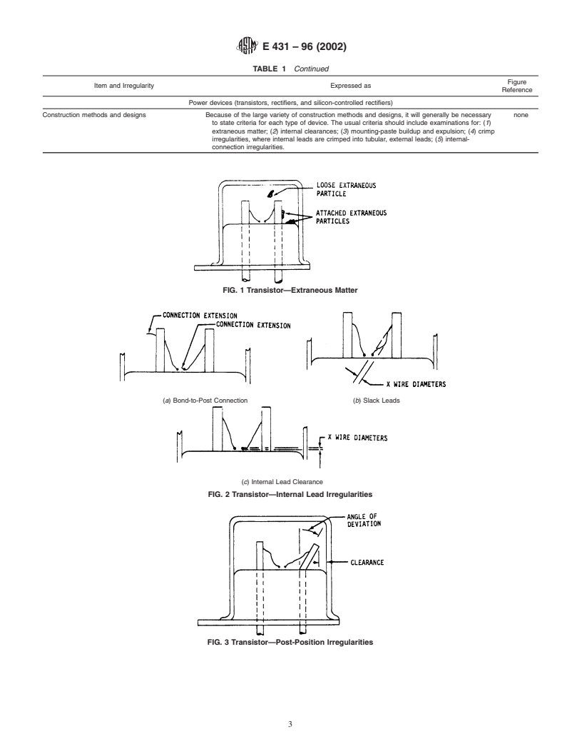
6.1 Description of irregularities and applicable figures are
shown in Table 1.
This guide is under the jurisdiction of ASTM Committee E07 on Nondestruc-
tive Testing and is the direct responsibility of Subcommittee E07.02 on Reference 7. Keywords
Radiological Images.
7.1 electronic devices; nondestructive testing; radiographs;
Current edition approved December 10, 1996. Published February 1997. Origi-
radiography; reference illustrations; semiconductors; x-ray
nally published as E 431 – 71. Last previous edition E 431 – 92.
Annual Book of ASTM Standards, Vol 03.03.
Copyright © ASTM International, 100 Barr Harbor Drive, PO Box C700, West Conshohocken, PA 19428-2959, United States.
E 431 – 96 (2002)
TABLE 1 Irregularity Description and Figure References
Figure
Item and Irregularity Expressed as
Reference
Transistors, low-power (TO-11 and smaller packages)
Extraneous matter Any material contained in the semiconductor device that is not necessary for its manufacture or 1
operation.
Internal lead irregularities, bond-to-post connection Leads extending beyond attachment points at either end. Allowable extension should be stated in 2(a)
wire diameters.
Slack leads deviate from a straight line between attachment points. Allowable deviation should 2(b)
be stated in wire diameters.
Internal lead clearance is the distance between the edge of the chip and lead wire. Allowable 2(c)
clearance should be stated in wire diameters.
Post-position irregularities Allowable deviations of the post from its intended (design) position may be specified as minimum 3
angle made by the post and header, or as clearance between post and post or post and case
expressed in terms of post diameter.
Getter-position irregularities In crimp-type devices, deviations of the getter ring from its intended (design) position are stated 4(a)
relative to the crimp. In noncrimp-type devices, deviations of the getter ring from its intended 4(b)
(design) position are stated as the angle between the actual and intended positions.
Mounting paste Mounting-paste buildup or expulsion, or both, is an excessive amount of material used to mount 5
the semiconductor element on the header. Allowable excess should be measured relative to
the surfaces, clearances, and shape of the deposit.
Post-connection solder or gold paste Post-connection solder or gold-paste buildup is an excessive amount of such material at the 6
termination. Excess is measured relative to the diameter at the attachment point and by the
deposit shape.
Diodes and low-power rectifiers (whisker-type)
Extraneous matter Any material contained in the cavity of the device that is not part of its design and not required 7(a)
for its manufacture or operation. 7(b)
7(c)
Whisker irregularities Any whisker malformation from its intended shape caused by compression. Allowable 8(a)
compression is stated as a percentage of design length.
Whisker cross-sectiona
...


Questions, Comments and Discussion
Ask us and Technical Secretary will try to provide an answer. You can facilitate discussion about the standard in here.