ASTM F3192-16
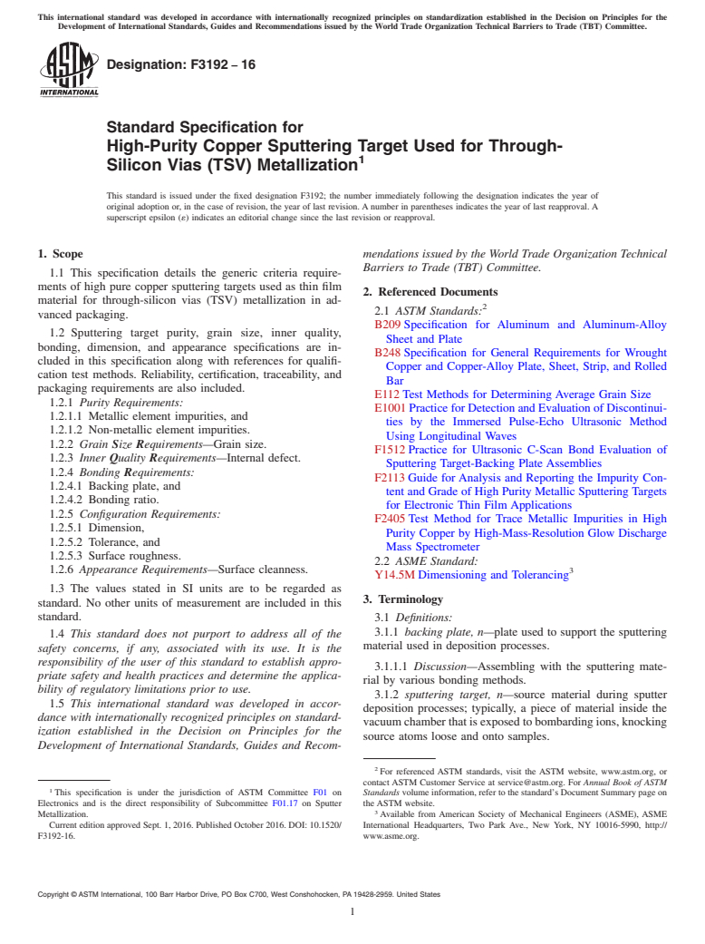
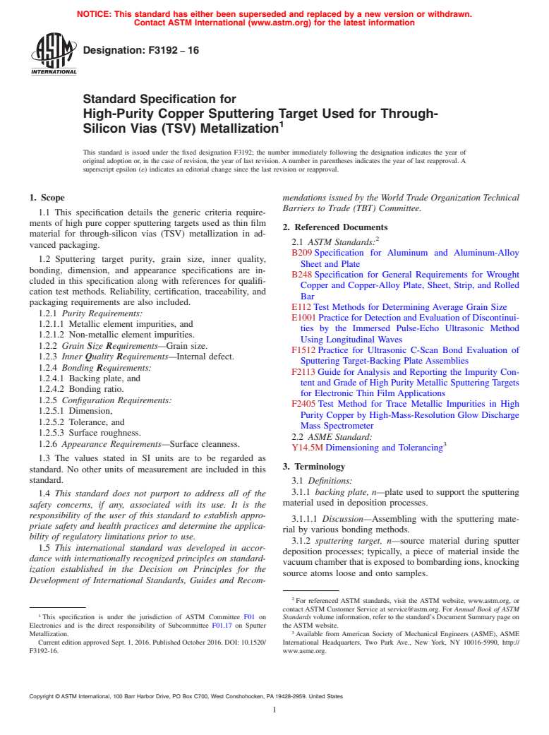
(Specification)Standard Specification for High-Purity Copper Sputtering Target Used for Through-Silicon Vias (TSV) Mettalization (Withdrawn 2023)
Standard Specification for High-Purity Copper Sputtering Target Used for Through-Silicon Vias (TSV) Mettalization (Withdrawn 2023)
ABSTRACT
This specification establishes the generic criteria requirements of high pure copper sputtering targets used as thin film material for through-silicon vias (TSV) metallization in advanced packaging. It covers purity (metallic and non-metallic element impurities), grain size, inner quality (internal defect), bonding (backing plate, bonding ratio), configuration (dimension, tolerance, surface roughness), and appearance (surface cleanness). It also includes sampling, traceability, reliability, certification, and packaging requirements.
SCOPE
1.1 This specification details the generic criteria requirements of high pure copper sputtering targets used as thin film material for through-silicon vias (TSV) metallization in advanced packaging.
1.2 Sputtering target purity, grain size, inner quality, bonding, dimension, and appearance specifications are included in this specification along with references for qualification test methods. Reliability, certification, traceability, and packaging requirements are also included.
1.2.1 Purity Requirements:
1.2.1.1 Metallic element impurities, and
1.2.1.2 Non-metallic element impurities.
1.2.2 Grain Size Requirements—Grain size.
1.2.3 Inner Quality Requirements—Internal defect.
1.2.4 Bonding Requirements:
1.2.4.1 Backing plate, and
1.2.4.2 Bonding ratio.
1.2.5 Configuration Requirements:
1.2.5.1 Dimension,
1.2.5.2 Tolerance, and
1.2.5.3 Surface roughness.
1.2.6 Appearance Requirements—Surface cleanness.
1.3 The values stated in SI units are to be regarded as standard. No other units of measurement are included in this standard.
1.4 This standard does not purport to address all of the safety concerns, if any, associated with its use. It is the responsibility of the user of this standard to establish appropriate safety and health practices and determine the applicability of regulatory limitations prior to use.
WITHDRAWN RATIONALE
This specification details the generic criteria requirements of high pure copper sputtering targets used as thin film material for through-silicon vias (TSV) metallization in advanced packaging.
Formerly under the jurisdiction of Committee F01 on Electronics, this specification was withdrawn in November 2023. This standard is being withdrawn without replacement because Committee F01 was disbanded.
General Information
Relations
Buy Standard
Standards Content (Sample)
This international standard was developed in accordance with internationally recognized principles on standardization established in the Decision on Principles for the
Development of International Standards, Guides and Recommendations issued by the World Trade Organization Technical Barriers to Trade (TBT) Committee.
Designation:F3192 −16
Standard Specification for
High-Purity Copper Sputtering Target Used for Through-
1
Silicon Vias (TSV) Metallization
This standard is issued under the fixed designation F3192; the number immediately following the designation indicates the year of
original adoption or, in the case of revision, the year of last revision. A number in parentheses indicates the year of last reapproval. A
superscript epsilon (´) indicates an editorial change since the last revision or reapproval.
1. Scope mendations issued by the World Trade Organization Technical
Barriers to Trade (TBT) Committee.
1.1 This specification details the generic criteria require-
ments of high pure copper sputtering targets used as thin film
2. Referenced Documents
material for through-silicon vias (TSV) metallization in ad-
2
2.1 ASTM Standards:
vanced packaging.
B209 Specification for Aluminum and Aluminum-Alloy
1.2 Sputtering target purity, grain size, inner quality,
Sheet and Plate
bonding, dimension, and appearance specifications are in-
B248 Specification for General Requirements for Wrought
cluded in this specification along with references for qualifi-
Copper and Copper-Alloy Plate, Sheet, Strip, and Rolled
cation test methods. Reliability, certification, traceability, and
Bar
packaging requirements are also included.
E112 Test Methods for Determining Average Grain Size
1.2.1 Purity Requirements:
E1001 Practice for Detection and Evaluation of Discontinui-
1.2.1.1 Metallic element impurities, and
ties by the Immersed Pulse-Echo Ultrasonic Method
1.2.1.2 Non-metallic element impurities.
Using Longitudinal Waves
1.2.2 Grain Size Requirements—Grain size.
F1512 Practice for Ultrasonic C-Scan Bond Evaluation of
1.2.3 Inner Quality Requirements—Internal defect.
Sputtering Target-Backing Plate Assemblies
1.2.4 Bonding Requirements:
F2113 Guide for Analysis and Reporting the Impurity Con-
1.2.4.1 Backing plate, and
tent and Grade of High Purity Metallic Sputtering Targets
1.2.4.2 Bonding ratio.
for Electronic Thin Film Applications
1.2.5 Configuration Requirements:
F2405 Test Method for Trace Metallic Impurities in High
1.2.5.1 Dimension,
Purity Copper by High-Mass-Resolution Glow Discharge
1.2.5.2 Tolerance, and
Mass Spectrometer
1.2.5.3 Surface roughness.
2.2 ASME Standard:
1.2.6 Appearance Requirements—Surface cleanness. 3
Y14.5M Dimensioning and Tolerancing
1.3 The values stated in SI units are to be regarded as
3. Terminology
standard. No other units of measurement are included in this
standard.
3.1 Definitions:
3.1.1 backing plate, n—plate used to support the sputtering
1.4 This standard does not purport to address all of the
material used in deposition processes.
safety concerns, if any, associated with its use. It is the
responsibility of the user of this standard to establish appro-
3.1.1.1 Discussion—Assembling with the sputtering mate-
priate safety and health practices and determine the applica-
rial by various bonding methods.
bility of regulatory limitations prior to use.
3.1.2 sputtering target, n—source material during sputter
1.5 This international standard was developed in accor-
deposition processes; typically, a piece of material inside the
dance with internationally recognized principles on standard-
vacuumchamberthatisexposedtobombardingions,knocking
ization established in the Decision on Principles for the
source atoms loose and onto samples.
Development of International Standards, Guides and Recom-
2
For referenced ASTM standards, visit the ASTM website, www.astm.org, or
contact ASTM Customer Service at service@astm.org. For Annual Book of ASTM
1
This specification is under the jurisdiction of ASTM Committee F01 on Standards volume information, refer to the standard’s Document Summary page on
Electronics and is the direct responsibility of Subcommittee F01.17 on Sputter the ASTM website.
3
Metallization. Available from American Society of Mechanical Engineers (ASME), ASME
Current edition approved Sept. 1, 2016. Published October 2016. DOI: 10.1520/ International Headquarters, Two Park Ave., New York, NY 10016-5990, http://
F3192-16. www.asme.org.
Copyright ©ASTM International, 100 Barr Harbor Drive, PO Box C700, West Conshohocken, PA19428-2959. United States
1
---------------------- Page: 1 ----------------------
F3192−16
3.1.2.1 Discussion—The sputtering target product can be weight (wt ppm). Additional elements may be analyzed and
classified as monolithic or assembly type according to the reported as agreed upon between the purchaser and the
configurations as shown in Fig. 1. supplier.
3.2 Definitions of Terms Specific to This Standard:
5.1.2 General acceptable analysis methods and detection
3.2.1 finishe
...
NOTICE: This standard has either been superseded and replaced by a new version or withdrawn.
Contact ASTM International (www.astm.org) for the latest information
Designation: F3192 − 16
Standard Specification for
High-Purity Copper Sputtering Target Used for Through-
1
Silicon Vias (TSV) Metallization
This standard is issued under the fixed designation F3192; the number immediately following the designation indicates the year of
original adoption or, in the case of revision, the year of last revision. A number in parentheses indicates the year of last reapproval. A
superscript epsilon (´) indicates an editorial change since the last revision or reapproval.
1. Scope mendations issued by the World Trade Organization Technical
Barriers to Trade (TBT) Committee.
1.1 This specification details the generic criteria require-
ments of high pure copper sputtering targets used as thin film
2. Referenced Documents
material for through-silicon vias (TSV) metallization in ad-
2
2.1 ASTM Standards:
vanced packaging.
B209 Specification for Aluminum and Aluminum-Alloy
1.2 Sputtering target purity, grain size, inner quality,
Sheet and Plate
bonding, dimension, and appearance specifications are in-
B248 Specification for General Requirements for Wrought
cluded in this specification along with references for qualifi-
Copper and Copper-Alloy Plate, Sheet, Strip, and Rolled
cation test methods. Reliability, certification, traceability, and
Bar
packaging requirements are also included.
E112 Test Methods for Determining Average Grain Size
1.2.1 Purity Requirements:
E1001 Practice for Detection and Evaluation of Discontinui-
1.2.1.1 Metallic element impurities, and
ties by the Immersed Pulse-Echo Ultrasonic Method
1.2.1.2 Non-metallic element impurities.
Using Longitudinal Waves
1.2.2 Grain Size Requirements—Grain size.
F1512 Practice for Ultrasonic C-Scan Bond Evaluation of
1.2.3 Inner Quality Requirements—Internal defect.
Sputtering Target-Backing Plate Assemblies
1.2.4 Bonding Requirements:
F2113 Guide for Analysis and Reporting the Impurity Con-
1.2.4.1 Backing plate, and
tent and Grade of High Purity Metallic Sputtering Targets
1.2.4.2 Bonding ratio.
for Electronic Thin Film Applications
1.2.5 Configuration Requirements:
F2405 Test Method for Trace Metallic Impurities in High
1.2.5.1 Dimension,
Purity Copper by High-Mass-Resolution Glow Discharge
1.2.5.2 Tolerance, and
Mass Spectrometer
1.2.5.3 Surface roughness.
2.2 ASME Standard:
1.2.6 Appearance Requirements—Surface cleanness. 3
Y14.5M Dimensioning and Tolerancing
1.3 The values stated in SI units are to be regarded as
3. Terminology
standard. No other units of measurement are included in this
standard.
3.1 Definitions:
3.1.1 backing plate, n—plate used to support the sputtering
1.4 This standard does not purport to address all of the
material used in deposition processes.
safety concerns, if any, associated with its use. It is the
responsibility of the user of this standard to establish appro-
3.1.1.1 Discussion—Assembling with the sputtering mate-
priate safety and health practices and determine the applica-
rial by various bonding methods.
bility of regulatory limitations prior to use.
3.1.2 sputtering target, n—source material during sputter
1.5 This international standard was developed in accor-
deposition processes; typically, a piece of material inside the
dance with internationally recognized principles on standard-
vacuum chamber that is exposed to bombarding ions, knocking
ization established in the Decision on Principles for the
source atoms loose and onto samples.
Development of International Standards, Guides and Recom-
2
For referenced ASTM standards, visit the ASTM website, www.astm.org, or
contact ASTM Customer Service at service@astm.org. For Annual Book of ASTM
1
This specification is under the jurisdiction of ASTM Committee F01 on Standards volume information, refer to the standard’s Document Summary page on
Electronics and is the direct responsibility of Subcommittee F01.17 on Sputter the ASTM website.
3
Metallization. Available from American Society of Mechanical Engineers (ASME), ASME
Current edition approved Sept. 1, 2016. Published October 2016. DOI: 10.1520/ International Headquarters, Two Park Ave., New York, NY 10016-5990, http://
F3192-16. www.asme.org.
Copyright © ASTM International, 100 Barr Harbor Drive, PO Box C700, West Conshohocken, PA 19428-2959. United States
1
---------------------- Page: 1 ----------------------
F3192 − 16
3.1.2.1 Discussion—The sputtering target product can be weight (wt ppm). Additional elements may be analyzed and
classified as monolithic or assembly type according to the reported as agreed upon between the purchaser and the
configurations as shown in Fig. 1. supplier.
3.2 Definitions of Terms Specific to This Standard:
5.1.2 General acceptable analysis methods and detection
3.2.1 finished product, n—for the purposes of this standard,
limits are specified in Guide F2113. Use Test Method F2405 to
a manufactured
...


Questions, Comments and Discussion
Ask us and Technical Secretary will try to provide an answer. You can facilitate discussion about the standard in here.