ISO 14606:2022
(Main)Surface chemical analysis — Sputter depth profiling — Optimization using layered systems as reference materials
Surface chemical analysis — Sputter depth profiling — Optimization using layered systems as reference materials
This document gives guidance and requirements on the optimization of sputter-depth profiling parameters using appropriate single-layered and multilayered reference materials, in order to achieve optimum depth resolution as a function of instrument settings in Auger electron spectroscopy, X-ray photoelectron spectroscopy and secondary ion mass spectrometry. This document is not intended to cover the use of special multilayered systems such as delta doped layers.
Analyse chimique des surfaces — Profilage d'épaisseur par bombardement — Optimisation à l'aide de systèmes mono- ou multicouches comme matériaux de référence
General Information
- Status
- Published
- Publication Date
- 20-Nov-2022
- Technical Committee
- ISO/TC 201/SC 4 - Depth profiling
- Drafting Committee
- ISO/TC 201/SC 4 - Depth profiling
- Current Stage
- 6060 - International Standard published
- Start Date
- 21-Nov-2022
- Due Date
- 17-Dec-2022
- Completion Date
- 21-Nov-2022
Relations
- Effective Date
- 18-Dec-2021
Overview
ISO 14606:2022 - "Surface chemical analysis - Sputter depth profiling - Optimization using layered systems as reference materials" provides guidance and requirements to optimize sputter depth profiling for surface chemical analysis. It specifies how to use single-layered and multilayered reference materials to achieve optimum depth resolution as a function of instrument settings in Auger electron spectroscopy (AES), X‑ray photoelectron spectroscopy (XPS) and secondary ion mass spectrometry (SIMS). The standard is explicit that special multilayer systems such as delta-doped layers are out of scope.
Key topics and requirements
- Optimization approach: Use of layered reference systems (single and multilayer) to evaluate and set instrument parameters for best depth resolution.
- Instrument families covered: AES, XPS, SIMS - including probing and sputtering parameter considerations for each technique.
- Critical parameters:
- Probing: electron/photon/primary ion energy, beam/current or source power, analysis area, emission angle.
- Sputtering: ion species, ion energy (typical range 0.1–25 keV in the standard), ion beam current (examples 1–10 nA), incidence angle, sputtered area and rastering.
- Measurement and metrics:
- Determination of average sputtering rate and the depth resolution (Δz) at an ideally sharp interface.
- Guidance on measuring depth resolution using layered references, and caveats for SIMS when matrix effects differ.
- Procedures and alignment:
- Practical procedures to align a sputtered crater with a smaller analysis area (including manufacturer-provided alignment tools).
- Stepwise optimization of parameter settings to balance analysis sensitivity versus depth resolution.
- Supporting material: Informative annexes on factors influencing depth resolution, typical reference single- and multilayer systems, and uses of multilayered systems.
Applications and users
ISO 14606:2022 is practical for:
- Surface analysts and lab technicians performing sputter depth profiling in AES, XPS and SIMS.
- Instrument manufacturers validating and demonstrating performance.
- Materials scientists and semiconductor engineers characterizing multilayer devices (e.g., optical/heterostructure devices) and coatings.
- Quality and metrology labs assessing depth profiling reproducibility and instrument settings.
Practical uses include optimizing ion beam conditions to reduce sputter-induced roughening, evaluating sample drift and crater geometry effects, and choosing suitable reference materials for method development.
Related standards
- Normative reference: ISO 18115-1 (Surface chemical analysis - Vocabulary).
- Developed by ISO/TC 201 (Surface chemical analysis) - useful alongside other ISO guidance on surface analysis and metrology.
Keywords: ISO 14606:2022, sputter depth profiling, surface chemical analysis, depth resolution, reference materials, AES, XPS, SIMS, ion sputtering.
Get Certified
Connect with accredited certification bodies for this standard

ECOCERT
Organic and sustainability certification.

Eurofins Food Testing Global
Global leader in food, environment, and pharmaceutical product testing.

Intertek Bangladesh
Intertek certification and testing services in Bangladesh.
Sponsored listings
Frequently Asked Questions
ISO 14606:2022 is a standard published by the International Organization for Standardization (ISO). Its full title is "Surface chemical analysis — Sputter depth profiling — Optimization using layered systems as reference materials". This standard covers: This document gives guidance and requirements on the optimization of sputter-depth profiling parameters using appropriate single-layered and multilayered reference materials, in order to achieve optimum depth resolution as a function of instrument settings in Auger electron spectroscopy, X-ray photoelectron spectroscopy and secondary ion mass spectrometry. This document is not intended to cover the use of special multilayered systems such as delta doped layers.
This document gives guidance and requirements on the optimization of sputter-depth profiling parameters using appropriate single-layered and multilayered reference materials, in order to achieve optimum depth resolution as a function of instrument settings in Auger electron spectroscopy, X-ray photoelectron spectroscopy and secondary ion mass spectrometry. This document is not intended to cover the use of special multilayered systems such as delta doped layers.
ISO 14606:2022 is classified under the following ICS (International Classification for Standards) categories: 71.040.40 - Chemical analysis. The ICS classification helps identify the subject area and facilitates finding related standards.
ISO 14606:2022 has the following relationships with other standards: It is inter standard links to ISO 14606:2015. Understanding these relationships helps ensure you are using the most current and applicable version of the standard.
ISO 14606:2022 is available in PDF format for immediate download after purchase. The document can be added to your cart and obtained through the secure checkout process. Digital delivery ensures instant access to the complete standard document.
Standards Content (Sample)
INTERNATIONAL ISO
STANDARD 14606
Third edition
2022-11
Surface chemical analysis — Sputter
depth profiling — Optimization using
layered systems as reference materials
Analyse chimique des surfaces — Profilage d'épaisseur par
bombardement — Optimisation à l'aide de systèmes mono- ou
multicouches comme matériaux de référence
Reference number
© ISO 2022
All rights reserved. Unless otherwise specified, or required in the context of its implementation, no part of this publication may
be reproduced or utilized otherwise in any form or by any means, electronic or mechanical, including photocopying, or posting on
the internet or an intranet, without prior written permission. Permission can be requested from either ISO at the address below
or ISO’s member body in the country of the requester.
ISO copyright office
CP 401 • Ch. de Blandonnet 8
CH-1214 Vernier, Geneva
Phone: +41 22 749 01 11
Email: copyright@iso.org
Website: www.iso.org
Published in Switzerland
ii
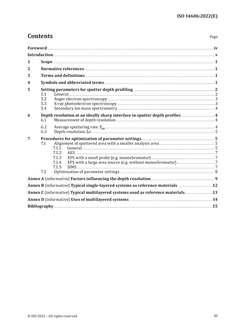
Contents Page
Foreword .iv
Introduction .v
1 Scope . 1
2 Normative references . 1
3 Terms and definitions . 1
4 Symbols and abbreviated terms.1
5 Setting parameters for sputter depth profiling . 2
5.1 General . 2
5.2 Auger electron spectroscopy . 3
5.3 X-ray photoelectron spectroscopy . 3
5.4 Secondary ion mass spectrometry . 4
6 Depth resolution at an ideally sharp interface in sputter depth profiles .4
6.1 Measurement of depth resolution . 4
6.2 Average sputtering rate z . 4
av
6.3 Depth resolution ∆z . 5
7 Procedures for optimization of parameter settings . 5
7.1 Alignment of sputtered area with a smaller analysis area . 5
7.1.1 General . 5
7.1.2 AES . 7
7.1.3 XPS with a small probe (e.g. monochromator) . 7
7.1.4 XPS with a large area source (e.g. without monochromator) . 7
7.1.5 SIMS . 7
7.2 Optimization of parameter settings . 8
Annex A (informative) Factors influencing the depth resolution . 9
Annex B (informative) Typical single-layered systems as reference materials .12
Annex C (informative) Typical multilayered systems used as reference materials .13
Annex D (informative) Uses of multilayered systems .14
Bibliography .15
iii
Foreword
ISO (the International Organization for Standardization) is a worldwide federation of national standards
bodies (ISO member bodies). The work of preparing International Standards is normally carried out
through ISO technical committees. Each member body interested in a subject for which a technical
committee has been established has the right to be represented on that committee. International
organizations, governmental and non-governmental, in liaison with ISO, also take part in the work.
ISO collaborates closely with the International Electrotechnical Commission (IEC) on all matters of
electrotechnical standardization.
The procedures used to develop this document and those intended for its further maintenance are
described in the ISO/IEC Directives, Part 1. In particular, the different approval criteria needed for the
different types of ISO documents should be noted. This document was drafted in accordance with the
editorial rules of the ISO/IEC Directives, Part 2 (see www.iso.org/directives).
Attention is drawn to the possibility that some of the elements of this document may be the subject of
patent rights. ISO shall not be held responsible for identifying any or all such patent rights. Details of
any patent rights identified during the development of the document will be in the Introduction and/or
on the ISO list of patent declarations received (see www.iso.org/patents).
Any trade name used in this document is information given for the convenience of users and does not
constitute an endorsement.
For an explanation of the voluntary nature of standards, the meaning of ISO specific terms and
expressions related to conformity assessment, as well as information about ISO's adherence to
the World Trade Organization (WTO) principles in the Technical Barriers to Trade (TBT), see
www.iso.org/iso/foreword.html.
This document was prepared by Technical Committee ISO/TC 201, Surface chemical analysis,
Subcommittee SC 4, Depth profiling.
This third edition cancels and replaces the second edition (ISO 14606:2015), which has been technically
revised.
The main changes are as follows:
— Clause 3: terms and definitions have been simplified using normative references;
— 6.2: descriptions have been added that it is only necessary to sputter off a few certain periods of
layers from the topmost surface to obtain average sputtering rate for practical use of a multi-layered
system;
— 7.1.3, 7.1.4 and 7.1.5: descriptions have been added to mention the use of the procedures provided by
manufacturer of apparatuses for alignment of sputtered area with a smaller analysis area;
— Table B.1 and Table C.1: contents have been updated.
Any feedback or questions on this document should be directed to the user’s national standards body. A
complete listing of these bodies can be found at www.iso.org/members.html.
iv
Introduction
Reference materials are useful in optimizing the depth resolution of sputter profiling methods in
materials such as silicon wafers, multilayered devices (e.g. AlGaAs double-hetero lasers, high electron
mobility transistors) and alloy-galvanized steel for corrosion-resistant car bodies.
The specific applications of this document are as follows.
a) Single-layered and multilayered systems on a substrate as reference materials are useful for
the optimization of depth resolution as a function of instrument settings in Auger electron
spectroscopy, X-ray photoelectron spectroscopy and secondary ion mass spectrometry.
b) These systems are useful for illustrating the effects of the evenness of the sputter crater, the
inclination of the crater bottom, the sample drift, the drift of sputter conditions (e.g. ion beam
current density) on depth resolution.
c) These systems are useful for illustrating the effects of sputter-induced surface roughening and
sputter-induced atomic mixing on depth resolution.
d) These systems are useful for the evaluation of instrument performance for instrument suppliers
and users.
e) This document is timely and topical, and can be used for a basis of future development of sputter
depth profiling.
[1][2][3][4][5]
A list of ISO Guides related to this document is given in the Bibliography .
v
INTERNATIONAL STANDARD ISO 14606:2022(E)
Surface chemical analysis — Sputter depth profiling —
Optimization using layered systems as reference materials
1 Scope
This document gives guidance and requirements on the optimization of sputter-depth profiling
parameters using appropriate single-layered and multilayered reference materials, in order to achieve
optimum depth resolution as a function of instrument settings in Auger electron spectroscopy, X-ray
photoelectron spectroscopy and secondary ion mass spectrometry.
This document is not intended to cover the use of special multilayered systems such as delta doped
layers.
2 Normative references
The following documents are referred to in the text in such a way that some or all of their content
constitutes requirements of this document. For dated references, only the edition cited applies. For
undated references, the latest edition of the referenced document (including any amendments) applies.
ISO 18115-1, Surface chemical analysis — Vocabulary — Part 1: General terms and terms used in
spectroscopy
3 Terms and definitions
For the purposes of this document, the terms and definitions given in ISO 18115-1 and the following
apply.
ISO and IEC maintain terminology databases for use in standardization at the following addresses:
— ISO Online browsing platform: available at https:// www .iso .org/ obp
— IEC Electropedia: available at https:// www .electropedia .org/
3.1
image depth profile
three-dimensional representation of the spatial distribution of a particular elemental or molecular
species (as indicated by emitted secondary ions or electrons) as a function of depth or material removed
by sputtering
3.2
plateau region
region in which the signal remains constant or without significant variation with sputtering time
3.3
sputter depth profile
depth profile obtained when the surface is measured as material is removed by sputtering
4 Symbols and abbreviated terms
∆z depth resolution
I signal intensity
z
sputtering rate
AES Auger electron spectroscopy
SEM scanning electron microscopy
SIMS secondary ion mass spectrometry
XPS X-ray photoelectron spectroscopy
5 Setting parameters for sputter depth profiling
5.1 General
For the purposes of this document, typical probing and sputtering parameters for sputter depth profiling
in AES, XPS and SIMS are given in Table 1 and Table 2. These parameters represent a range which covers
many different types of instrumentation. Recommended conditions for a particular instrument may
be available from the respective instrument manufacturers and optimized by experimentation on the
laboratory instrument using the information included in this document.
Table 1 — Typical probing parameters for sputter depth profiling
AES XPS SIMS
Probing species Electrons Photons: Primary ions:
+ – + +
Mg Kα, Al Kα Cs , O , O , Ga
Energy of probing 1 keV to 25 keV 1,253 keV, 1,486 keV 0,1 keV to 25 keV
species
3 4 4
Current or power 1 nA to 10 nA 1 W to 10 W 1 nA to 10 nA
(Faraday cup) (Source power) (Faraday cup)
Angle of incidence 0° ≤ θ < 90° 0° ≤ θ < 90° 0° ≤ θ < 90°
Analysed species Auger electrons in eV Photoelectrons in eV Secondary ions in AMU
(kinetic energy) (kinetic or binding energy) (mass or mass/charge)
Energy range of emis- 0 keV to 3 keV 0 keV to 1,5 keV 0 keV to 0,125 keV
sion species
Angle of emission 0° ≤ θ< 90° 0° ≤ θ < 90° 0° ≤ θ < 90°
−8 2 −2 2 −4 2 2 −6 2 −2 2
Analysis area 10 mm to 10 mm 10 mm to 10 mm 10 mm to 10 mm
Table 2 — Typical sputtering parameters for sputter depth profiling
Typical operating parameters Remarks
+ + + – + + +
Ion species Ar , Kr , Xe , O , O , Ga , Cs Inert or reactive gas ions or metal ions
Ion energy 0,1 keV to 25 keV
Ion beam current 1 nA to 10 nA Faraday cup
Angle of incidence 0° ≤ θ < 90°
−2 2 2 2
Sputtered area 10 mm to 10 mm Raster scan of focused ion beam
NOTE The ion gun parameters and vacuum conditions can also affect the depth resolution. For example, the
gas pressure in the ion source can change during the course of the analysis.
5.2 Auger electron spectroscopy
Important parameters for a depth profile measurement of a single layered or an A/B/A/B/. multilayered
[6]
system by AES with ion sputtering are the following .
a) Probing parameters (important for analysis): Electron energy, electron beam current, angle of
incidence, analysis area (i.e. beam diameter or raster area).
b) Sputtering parameters (important for depth resolution): Ion species, ion energy, ion beam
[7]
current , angle of incidence, sputtered or raster area. Sample stage is in a stationary or rotational
mode.
c) Measurement parameters:
1) Kinetic energies of Auger electrons from both overlayer and substrate elements, or from
elements A and B (important for both analysis and depth resolution).
2) Direct mode, N (E) or EN (E), or differential mode, dN (E)/dE or dEN (E)/dE (important for
analysis).
NOTE 1 N(E), EN(E), dN(E)/dE and dEN(E)/dE refer to different kinds of Auger spectra
where the Auger electron intensity, N, is plotted as a function of the electron kinetic energy, E. In
N(E) spectra, signal intensities are measured as the heights of the Auger peaks above background. In
dN(E)/dE spectra, signal intensities are measured as the peak-to-peak heights of the Auger signals or
the differential spectra of N(E). With certain types of analyser (e.g. the cylindrical mirror analyser),
Auger electron intensities are presented in EN(E) and dEN(E)/dE formats, in which the spectrum
approximates E times N(E).
3) With ion sputtering, data may be collected in either an alternating mode or continuous mode.
If the continuous mode is used, it is preferable to ensure that the ion-induced Auger electron
signals are negligible.
NOTE 2 The problem of ion-induced Auger electrons seems only significant for Auger electron
[8][9]
peaks below 100 eV .
5.3 X-ray photoelectron spectroscopy
Important parameters for a depth profile measurement of a single layered or an A/B/A/B/. multilayered
system by XPS with ion sputtering are the following.
a) Probing parameters (important for analysis): Photon energy (X-ray source), X-ray source power
(i.e. voltage and current), angle of incidence, analysis area (i.e. beam diameter or selected area).
b) Sputtering parameters (important for depth resolution): Ion species, ion energy, ion beam current,
angle of incidence, sputtered or raster area. The sample stage can be in a stationary or rotational
mode.
c) Measurement parameters (important for both analysis and depth resolution):
1) kinetic energies of photoelectrons and/or the respective electron binding energies of both
overlayer and substrate elements or both elements A and B;
2) area of measurement for selected area XPS;
3) emission angle of electrons.
NOTE Usually, XPS signal intensities are measured as a function of sputtering time in an alternating mode
with ion sputtering.
5.4 Secondary ion mass spectrometry
Important parameters for a depth profile measurement of a single layered or an A/B/A/B/. multilayered
system by SIMS are the following.
a) Probing and simultaneously sputtering parameters (important for both analysis and depth
resolution): Primary ion species, ion impact energy, ion beam current, angle of incidence, analysis
area (i.e. gated area), sputtered area. The sample stage can be a stationary or rotational mode.
NOTE 1 In some SIMS systems, the beam energy is given for the source potential with respect to the
ground but the sample potential is not at ground. The impact energy takes account of the sample potential.
NOTE 2 Some time-of-flight SIMS instruments use dual beams. In this case, all parameters for both beams
are noted.
b) Measurement parameters (important for both analysis and depth resolution):
1) positive or negative secondary ion species (atomic or molecular) of both overlayer and
substrate elements or both elements A and B;
2) settings of gates (i.e. electronic, optical, etc.).
NOTE 3 Usually, secondary ion signal intensities are measured as a function of sputtering time in a continuous
mode with primary ion sputtering. In some SIMS instruments, an interrupted mode (primary ion gating) is used
where different ion beams are used for sputtering and analysis.
6 Depth resolution at an ideally sharp interface in sputter depth profiles
6.1 Measurement of depth resolution
For the purposes of this document, the measurement of the depth resolution ∆z of sputter depth profiles
[10][11][12]
of a single layered or an A/B/A/B/. multilayered system is as follows .
For SIMS, where matrix effects are significantly different between the two layers, ∆z may still be used
for optimization but may not relate closely to the real depth resolution of the underlying chemical
composition.
NOTE The definition of depth resolution ∆z in this clause applies only for optimization of setting parameters
in depth profiling. The definition and measurement procedures of depth resolution will be described in
International Standards to be developed by ISO/TC 201/SC 1 and SC 4, respectively, in the future.
6.2 Average sputtering rate z
av
The average sputtering rate z is given by Formula (1):
av
z = z /t (1)
av tot tot
where
z is the total thickness of a single overlayer or multilayered system on a substrate;
tot
t is the total sputtering time required to sputter from the topmost surface until the overlay-
tot
er/substrate interface at which the signal intensity of the element reaches 50 % of its value
in the adjacent overlayer on a substrate.
In practical cases using a multilayered system, the total thickness of a few certain periods of layers
from the topmost surface and the time required to sputter from the topmost surface until the
corresponding interface between the final layer of the certain periods of layers and the layer below
them may be used as z and t , respectively, to obtain z .
tot tot av
6.3 Depth resolution ∆z
Depth resolution, ∆z, is given by Formula (2):
∆z = z × ∆t (2)
av
where ∆t is the sputtering time interval in which the signal intensities change from 16 % to 84 % (or
84 % to 16 %) of the intensity corresponding to 100 % of each of the overlayer and the substrate of a
single-layered system or each of the adjacent layers of a multilayer system.
The measurement of ∆t is only applicable where plateau regions have been obtained for both maximum
and minimum intensities (see Figure 1).
Key
I signal intensity
t sputtering time
a
Plateau region.
Figure 1 — Diagram of the measurement of ∆t at an ideally sharp interface in a sputter
depth profile
7 Procedures for optimization of parameter settings
7.1 Alignment of sputtered area with a smaller analysis area
7.1.1 General
The centre of a sputtered area shall be aligned with a smaller analysis area using an appropriate
method. The ratio of the analysis area to the sputtered area should be chosen to be as small as possible
[15]
so as to reduce effects resulting in the depth resolution due to the proximity to the crater edge . A
number of different situations exist, as shown in Figure 2.
a) b)
c) d)
Key
1 sample
2 probe
3 sputtered area
4 direction of ions
5 spectrometer analysis area
6 elect
...


Questions, Comments and Discussion
Ask us and Technical Secretary will try to provide an answer. You can facilitate discussion about the standard in here.
Loading comments...