ASTM F1620-96
(Practice)Standard Practice for Calibrating a Scanning Surface Inspection System Using Monodisperse Polystyrene Latex Spheres Deposited on Polished or Epitaxial Wafer Surfaces (Withdrawn 2003)
Standard Practice for Calibrating a Scanning Surface Inspection System Using Monodisperse Polystyrene Latex Spheres Deposited on Polished or Epitaxial Wafer Surfaces (Withdrawn 2003)
SCOPE
This standard was transferred to SEMI (www.semi.org) May 2003
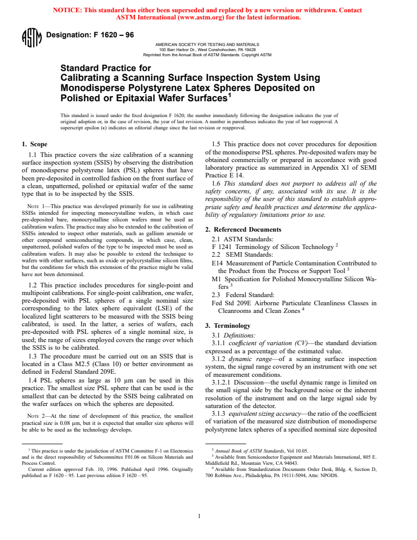
1.1 This practice covers the size calibration of a scanning surface inspection system (SSIS) by observing the distribution of monodisperse polystyrene latex (PSL) spheres that have been pre-deposited in controlled fashion on the front surface of a clean, unpatterned, polished or epitaxial wafer of the same type that is to be inspected by the SSIS. Note 1-This practice was developed primarily for use in calibrating SSISs intended for inspecting monocrystalline wafers, in which case pre-deposited bare, monocrystalline silicon wafers must be used as calibration wafers. The practice may also be extended to the calibration of SSISs intended to inspect other materials, such as gallium arsenide or other compound semiconducting compounds, in which case, clean, unpatterned, polished wafers of the type to be inspected must be used as calibration wafers. It may also be possible to extend the technique to wafers with other surfaces, such as oxide or polycrystalline silicon films, but the conditions for which this extension of the practice might be valid have not been determined.
1.2 This practice includes procedures for single-point and multipoint calibrations. For single-point calibration, one wafer, pre-deposited with PSL spheres of a single nominal size corresponding to the latex sphere equivalent (LSE) of the localized light scatterers to be measured with the SSIS being calibrated, is used. In the latter, a series of wafers, each pre-deposited with PSL spheres of a single nominal size, is used; the range of sizes employed covers the range over which the SSIS is to be calibrated.
1.3 The procedure must be carried out on an SSIS that is located in a Class M2.5 (Class 10) or better environment as defined in Federal Standard 209E.
1.4 PSL spheres as large as 10 [mu]m can be used in this practice. The smallest size PSL sphere that can be used is the smallest that can be detected by the SSIS being calibrated on the wafer surfaces on which the spheres are deposited. Note 2-At the time of development of this practice, the smallest practical size is 0.08 [mu]m, but it is expected that smaller size spheres will be able to be used as the technology develops.
1.5 This practice does not cover procedures for deposition of the monodisperse PSL spheres. Pre-deposited wafers may be obtained commercially or prepared in accordance with good laboratory practice as summarized in Appendix A1 of SEMI Practice E14.
1.6 This standard does not purport to address all of the safety concerns, if any, associated with its use. It is the responsibility of the user of this standard to establish appropriate safety and health practices and determine the applicability of regulatory limitations prior to use.
General Information
Standards Content (Sample)
NOTICE: This standard has either been superseded and replaced by a new version or withdrawn. Contact
ASTM International (www.astm.org) for the latest information.
Designation: F 1620 – 96
AMERICAN SOCIETY FOR TESTING AND MATERIALS
100 Barr Harbor Dr., West Conshohocken, PA 19428
Reprinted from the Annual Book of ASTM Standards. Copyright ASTM
Standard Practice for
Calibrating a Scanning Surface Inspection System Using
Monodisperse Polystyrene Latex Spheres Deposited on
1
Polished or Epitaxial Wafer Surfaces
This standard is issued under the fixed designation F 1620; the number immediately following the designation indicates the year of
original adoption or, in the case of revision, the year of last revision. A number in parentheses indicates the year of last reapproval. A
superscript epsilon (e) indicates an editorial change since the last revision or reapproval.
1. Scope 1.5 This practice does not cover procedures for deposition
of the monodisperse PSL spheres. Pre-deposited wafers may be
1.1 This practice covers the size calibration of a scanning
obtained commercially or prepared in accordance with good
surface inspection system (SSIS) by observing the distribution
laboratory practice as summarized in Appendix X1 of SEMI
of monodisperse polystyrene latex (PSL) spheres that have
Practice E 14.
been pre-deposited in controlled fashion on the front surface of
1.6 This standard does not purport to address all of the
a clean, unpatterned, polished or epitaxial wafer of the same
safety concerns, if any, associated with its use. It is the
type that is to be inspected by the SSIS.
responsibility of the user of this standard to establish appro-
NOTE 1—This practice was developed primarily for use in calibrating
priate safety and health practices and determine the applica-
SSISs intended for inspecting monocrystalline wafers, in which case
bility of regulatory limitations prior to use.
pre-deposited bare, monocrystalline silicon wafers must be used as
calibration wafers. The practice may also be extended to the calibration of
2. Referenced Documents
SSISs intended to inspect other materials, such as gallium arsenide or
2.1 ASTM Standards:
other compound semiconducting compounds, in which case, clean,
2
unpatterned, polished wafers of the type to be inspected must be used as
F 1241 Terminology of Silicon Technology
calibration wafers. It may also be possible to extend the technique to
2.2 SEMI Standards:
wafers with other surfaces, such as oxide or polycrystalline silicon films,
E14 Measurement of Particle Contamination Contributed to
but the conditions for which this extension of the practice might be valid
3
the Product from the Process or Support Tool
have not been determined.
M1 Specification for Polished Monocrystalline Silicon Wa-
3
1.2 This practice includes procedures for single-point and
fers
multipoint calibrations. For single-point calibration, one wafer,
2.3 Federal Standard:
pre-deposited with PSL spheres of a single nominal size
Fed Std 209E Airborne Particulate Cleanliness Classes in
corresponding to the latex sphere equivalent (LSE) of the 4
Cleanrooms and Clean Zones
localized light scatterers to be measured with the SSIS being
calibrated, is used. In the latter, a series of wafers, each
3. Terminology
pre-deposited with PSL spheres of a single nominal size, is
3.1 Definitions:
used; the range of sizes employed covers the range over which
3.1.1 coeffıcient of variation (CV)—the standard deviation
the SSIS is to be calibrated.
expressed as a percentage of the estimated value.
1.3 The procedure must be carried out on an SSIS that is
3.1.2 dynamic range—of a scanning surface inspection
located in a Class M2.5 (Class 10) or better environment as
system, the signal range covered by an instrument with one set
defined in Federal Standard 209E.
of measurement conditions.
1.4 PSL spheres as large as 10 μm can be used in this
3.1.2.1 Discussion—the useful dynamic range is limited on
practice. The smallest size PSL sphere that can be used is the
the small signal side by the background noise or the inherent
smallest that can be detected by the SSIS being calibrated on
resolution of the instrument and on the large signal side by
the wafer surfaces on which the spheres are deposited.
saturation of the detector.
3.1.3 equivalent sizing accuracy—the ratio of the coefficient
NOTE 2—At the time of development of this practice, the smallest
of variation of the measured size distribution of monodisperse
practical size is 0.08 μm, but it is expected that smaller size spheres will
be able to be used as the technology develops. polystyrene latex spheres of a specified nominal size deposited
1 2
This practice is under the jurisdiction of ASTM Committee F-1 on Electronics Annual Book of ASTM Standards, Vol 10.05.
3
and is the direct responsibility of Subcommittee F01.06 on Silicon Materials and Available from Semiconductor Equipment and Materials International, 805 E.
Process Control. Middlefield Rd., Mountain View, CA 94043.
4
...


Questions, Comments and Discussion
Ask us and Technical Secretary will try to provide an answer. You can facilitate discussion about the standard in here.