ASTM F1529-02
(Test Method)Standard Test Method for Sheet Resistance Uniformity Evaluation by In-Line Four-Point Probe with the Dual-Configuration Procedure
Standard Test Method for Sheet Resistance Uniformity Evaluation by In-Line Four-Point Probe with the Dual-Configuration Procedure
SCOPE
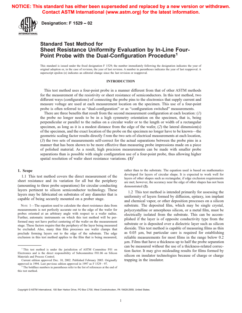
1.1 This test method covers the direct measurement of the sheet resistance and its variation for all but the periphery (amounting to three probe separations) for circular conducting layers pertinent to silicon semiconductor technology. These layers may be fabricated on substrates of any diameter that is capable of being securely mounted on a prober stage.
Note 1—The equation used to calculate the sheet resistance data from measurements is not perfectly accurate out to the edge of the wafer for probes oriented at an arbitrary angle with respect to a wafer radius. Further, automatic instruments on which this test method will be performed may not have perfect centering of the wafer on the measurement stage. These factors require that the periphery of the layer being measured be excluded. Also, many thin film processes use wafer clamps that preclude forming layers out to the edge of the substrate. The edge exclusion in this test method applies to the film that is being measured, rather than to the substrate. The equation used is based on mathematics developed for layers of circular shape. It is expected to work well for layers of other shapes such as rectangular, if edge exclusion requirements are met; however, the accuracy near the edge of other shapes has not been demonstrated (2).
1.2 This test method is intended primarily for assessing the uniformity of layers formed by diffusion, epitaxy, ion implant and chemical vapor, or other deposition processes on a silicon substrate. The deposited film, which may be single crystal, polycrystalline or amorphous silicon, or a metal film, must be electrically isolated from the substrate. This can be accomplished if the layer is of opposite conductivity type from the substrate or is deposited over a dielectric layer such as silicon dioxide. This test method is capable of measuring films as thin as 0.05 m, but particular care is required for establishing reliable measurements for most films in the range below 0.2 m. Films that have a thickness up to half the probe separation can be measured without the use of a thickness-related correction factor. It may give misleading results for films formed by silicon on insulator technologies because of charge or charge trapping in the insulator.
1.3 This test method can be used to measure the sheet resistance uniformity of bulk substrates. However, the thickness of the substrate must be known to be constant or must be measured at all positions where sheet resistance values are measured in order to calculate relative variations in resistance reliably.
Note 2—The thickness correction factor for layers that are thicker than 0.5 times the probe spacing is known to vary more rapidly than that for single-configuration four-probe measurements, but such a correction has not yet been published. Until such a correction is published, resistivity values determined by the dual-configuration method will not be accurate for these thicker specimens; however, if the wafer has uniform thickness, variations of resistivity can still be determined by this test method.
1.4 This test method can be used to measure sheet resistance values from below 10 m for metal films, to over 25 000 for thin silicon films. However, for films at the upper end of this resistance range, and for films toward the low end of the thickness range, the interpretation of the sheet resistance values may not be straightforward due to various semiconductor effects (3, 4, 5).
Note 3—The principles of this test method are also applicable to other semiconductor materials, but the appropriate conditions and the expected precision have not been established.
1.5 This test method uses two different electrical configurations of the four-point probe at each measurement location. It does not require measurement of probe location on the wafer, or probe separations, or of wafer diameter (except to determine edge exclusion for measurement-site selection) as do other four-point probe methods...
General Information
Relations
Standards Content (Sample)
NOTICE: This standard has either been superseded and replaced by a new version or withdrawn.
Contact ASTM International (www.astm.org) for the latest information.
Designation: F 1529 – 02
Standard Test Method for
Sheet Resistance Uniformity Evaluation by In-Line Four-
1
Point Probe with the Dual-Configuration Procedure
This standard is issued under the fixed designation F 1529; the number immediately following the designation indicates the year of
original adoption or, in the case of revision, the year of last revision. A number in parentheses indicates the year of last reapproval. A
superscript epsilon (e) indicates an editorial change since the last revision or reapproval.
INTRODUCTION
This test method uses a four-point probe in a manner different from that of other ASTM methods
for the measurement of the resistivity or sheet resistance of semiconductors. In this test method, two
different ways (configurations) of connecting the probe pins to the electronics that supply current and
measure voltage are used at each measurement location on the specimen. This use of a four-point
probe is often referred to as “dual-configuration” or as “configuration switched” measurements.
There are three benefits that result from the second measurement configuration at each location: (1)
the probe no longer needs to be in a high symmetry orientation on the specimen, that is, being
perpendicular or parallel to the radius on a circular wafer or to the length or width of a rectangular
specimen, as long as it is a modest distance from the edge of the wafer, (2) the lateral dimension(s)
of the specimen, and the exact location of the probe on the specimen no longer have to be known—the
geometric scaling factor results directly f rom the two sets of electrical measurements at each location,
(3) the two sets of measurements self-correct for the actual separations between the probe pins in a
manner that has been shown to be more effective than measuring probe impressions made on a piece
of polished material. As a result, high precision measurements can be made with smaller probe
separations than is possible with single configuration use of a four-point probe, thus allowing higher
2
spatial resolution of wafer sheet resistance variations. (1)
rather than to the substrate. The equation used is based on mathematics
1. Scope
developed for layers of circular shape. It is expected to work well for
1.1 This test method covers the direct measurement of the
layers of other shapes such as rectangular, if edge exclusion requirements
sheet resistance and its variation for all but the periphery
are met; however, the accuracy near the edge of other shapes has not been
(amounting to three probe separations) for circular conducting
demonstrated (2).
layers pertinent to silicon semiconductor technology. These
1.2 This test method is intended primarily for assessing the
layers may be fabricated on substrates of any diameter that is
uniformity of layers formed by diffusion, epitaxy, ion implant
capable of being securely mounted on a prober stage.
and chemical vapor, or other deposition processes on a silicon
NOTE 1—The equation used to calculate the sheet resistance data from substrate. The deposited film, which may be single crystal,
measurements is not perfectly accurate out to the edge of the wafer for
polycrystalline or amorphous silicon, or a metal film, must be
probes oriented at an arbitrary angle with respect to a wafer radius.
electrically isolated from the substrate. This can be accom-
Further, automatic instruments on which this test method will be per-
plished if the layer is of opposite conductivity type from the
formed may not have perfect centering of the wafer on the measurement
substrate or is deposited over a dielectric layer such as silicon
stage. These factors require that the periphery of the layer being measured
dioxide. This test method is capable of measuring films as thin
be excluded. Also, many thin film processes use wafer clamps that
as 0.05 μm, but particular care is required for establishing
preclude forming layers out to the edge of the substrate. The edge
exclusion in this test method applies to the film that is being measured,
reliable measurements for most films in the range below 0.2
μm. Films that have a thickness up to half the probe separation
can be measured without the use of a thickness-related correc-
1
This test method is under the jurisdiction of ASTM Committee F01 on
tion factor. It may give misleading results for films formed by
Electronics and is the direct responsibility of Subcommittee F01.06 on Silicon
silicon on insulator technologies because of charge or charge
Materials and Process Control.
Current edition approved Dec. 10, 2002. Published February 2003. Originally trapping in the insulator.
approved in 1994. Last previous edition approved in 1997 as F 1529 – 97.
2
The boldface numbers in parentheses refer to the list of references at the end of
this test method.
Copyright © ASTM International, 100 Barr Harbor Dr
...


Questions, Comments and Discussion
Ask us and Technical Secretary will try to provide an answer. You can facilitate discussion about the standard in here.