ASTM F978-02
(Test Method)Standard Test Method for Characterizing Semiconductor Deep Levels by Transient Capacitance Techniques (Withdrawn 2003)
Standard Test Method for Characterizing Semiconductor Deep Levels by Transient Capacitance Techniques (Withdrawn 2003)
SCOPE
This standard was transferred to SEMI (www.semi.org) May 2003
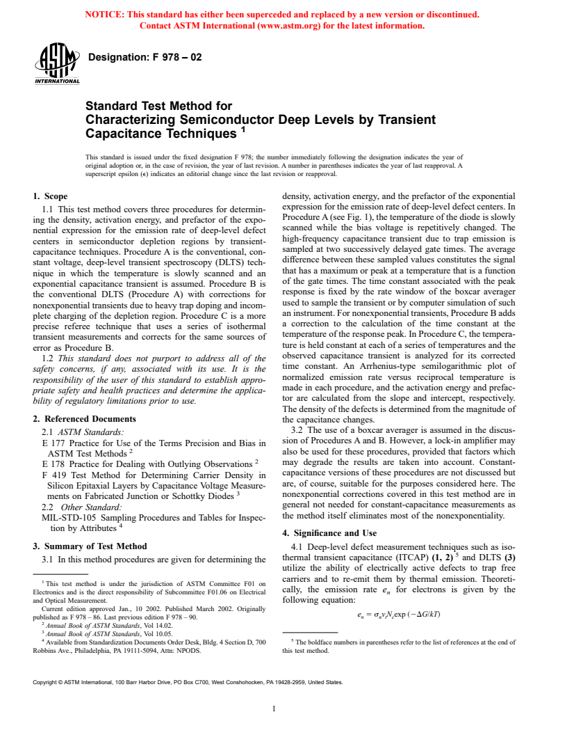
1.1 This test method covers three procedures for determining the density, activation energy, and prefactor of the exponential expression for the emission rate of deep-level defect centers in semiconductor depletion regions by transient-capacitance techniques. Procedure A is the conventional, constant voltage, deep-level transient spectroscopy (DLTS) technique in which the temperature is slowly scanned and an exponential capacitance transient is assumed. Procedure B is the conventional DLTS (Procedure A) with corrections for nonexponential transients due to heavy trap doping and incomplete charging of the depletion region. Procedure C is a more precise referee technique that uses a series of isothermal transient measurements and corrects for the same sources of error as Procedure B.
1.2 This standard does not purport to address all of the safety concerns, if any, associated with its use. It is the responsibility of the user of this standard to establish appropriate safety and health practices and determine the applicability of regulatory limitations prior to use.
General Information
Relations
Standards Content (Sample)
NOTICE: This standard has either been superceded and replaced by a new version or discontinued.
Contact ASTM International (www.astm.org) for the latest information.
Designation: F 978 – 02
Standard Test Method for
Characterizing Semiconductor Deep Levels by Transient
1
Capacitance Techniques
This standard is issued under the fixed designation F 978; the number immediately following the designation indicates the year of
original adoption or, in the case of revision, the year of last revision. A number in parentheses indicates the year of last reapproval. A
superscript epsilon (e) indicates an editorial change since the last revision or reapproval.
1. Scope density, activation energy, and the prefactor of the exponential
expression for the emission rate of deep-level defect centers. In
1.1 This test method covers three procedures for determin-
Procedure A (see Fig. 1), the temperature of the diode is slowly
ing the density, activation energy, and prefactor of the expo-
scanned while the bias voltage is repetitively changed. The
nential expression for the emission rate of deep-level defect
high-frequency capacitance transient due to trap emission is
centers in semiconductor depletion regions by transient-
sampled at two successively delayed gate times. The average
capacitance techniques. Procedure A is the conventional, con-
difference between these sampled values constitutes the signal
stant voltage, deep-level transient spectroscopy (DLTS) tech-
that has a maximum or peak at a temperature that is a function
nique in which the temperature is slowly scanned and an
of the gate times. The time constant associated with the peak
exponential capacitance transient is assumed. Procedure B is
response is fixed by the rate window of the boxcar averager
the conventional DLTS (Procedure A) with corrections for
used to sample the transient or by computer simulation of such
nonexponential transients due to heavy trap doping and incom-
an instrument. For nonexponential transients, Procedure B adds
plete charging of the depletion region. Procedure C is a more
a correction to the calculation of the time constant at the
precise referee technique that uses a series of isothermal
temperature of the response peak. In Procedure C, the tempera-
transient measurements and corrects for the same sources of
ture is held constant at each of a series of temperatures and the
error as Procedure B.
observed capacitance transient is analyzed for its corrected
1.2 This standard does not purport to address all of the
time constant. An Arrhenius-type semilogarithmic plot of
safety concerns, if any, associated with its use. It is the
normalized emission rate versus reciprocal temperature is
responsibility of the user of this standard to establish appro-
made in each procedure, and the activation energy and prefac-
priate safety and health practices and determine the applica-
tor are calculated from the slope and intercept, respectively.
bility of regulatory limitations prior to use.
The density of the defects is determined from the magnitude of
2. Referenced Documents
the capacitance changes.
3.2 The use of a boxcar averager is assumed in the discus-
2.1 ASTM Standards:
sion of Procedures A and B. However, a lock-in amplifier may
E 177 Practice for Use of the Terms Precision and Bias in
2
also be used for these procedures, provided that factors which
ASTM Test Methods
2
may degrade the results are taken into account. Constant-
E 178 Practice for Dealing with Outlying Observations
capacitance versions of these procedures are not discussed but
F 419 Test Method for Determining Carrier Density in
are, of course, suitable for the purposes considered here. The
Silicon Epitaxial Layers by Capacitance Voltage Measure-
3
nonexponential corrections covered in this test method are in
ments on Fabricated Junction or Schottky Diodes
general not needed for constant-capacitance measurements as
2.2 Other Standard:
the method itself eliminates most of the nonexponentiality.
MIL-STD-105 Sampling Procedures and Tables for Inspec-
4
tion by Attributes
4. Significance and Use
3. Summary of Test Method
4.1 Deep-level defect measurement techniques such as iso-
5
thermal transient capacitance (ITCAP) (1, 2) and DLTS (3)
3.1 In this method procedures are given for determining the
utilize the ability of electrically active defects to trap free
carriers and to re-emit them by thermal emission. Theoreti-
1
This test method is under the jurisdiction of ASTM Committee F01 on
cally, the emission rate e for electrons is given by the
Electronics and is the direct responsibility of Subcommittee F01.06 on Electrical n
and Optical Measurement. following equation:
Current edition approved Jan., 10 2002. Published March 2002. Originally
e 5s v N exp ~2DG/kT!
n n t c
published as F 978 – 86. Last previous edition F 978 – 90.
2
Annual Book of ASTM Standards, Vol 14.02.
3
Annual Book of ASTM Standards, Vol 10.05.
4 5
Available from Standardization Documents Order Desk, Bldg. 4 Section
...


Questions, Comments and Discussion
Ask us and Technical Secretary will try to provide an answer. You can facilitate discussion about the standard in here.