ASTM F1810-97
(Test Method)Standard Test Method for Counting Preferentially Etched or Decorated Surface Defects in Silicon Wafers
Standard Test Method for Counting Preferentially Etched or Decorated Surface Defects in Silicon Wafers
SCOPE
1.1 This test method describes the technique to count the density of surface defects in silicon wafers by microscopic analysis.
Note 1-Practical use of a defect counting method requires an assumption be made that defects are randomly distributed on the surface. If this assumption is not met, the accuracy and precision of this test method will be diminished.
1.2 Application of this test method is limited to specimens that have discrete, identifiable artifacts on the surface of the silicon sample. Typical samples have been preferentially etched according to Guide F 1809 or epitaxially deposited, forming defects in a silicon layer structure.
1.3 Wafer thickness and diameter for this test method is limited only by the range or microscope stage motions available.
1.4 This test method is applicable to silicon wafers with defect density between 0.01 and 10 000 defects per cm2.
Note 2-The commercially significant defect density range is between 0.01 to 10 defects per cm2, but this test method extends to higher defect levels due to improved statistical sampling obtained with higher counts.
1.5 This standard does not purport to address all of the safety concerns, if any, associated with its use. It is the responsibility of the user of this standard to establish appropriate safety and health practices and determine the applicability of regulatory limitations prior to use.
General Information
Relations
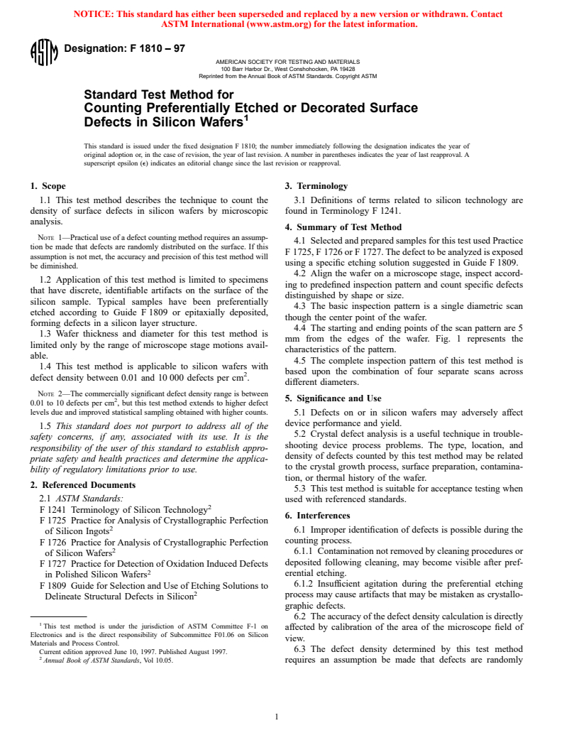
Standards Content (Sample)
NOTICE: This standard has either been superseded and replaced by a new version or withdrawn. Contact
ASTM International (www.astm.org) for the latest information.
Designation: F 1810 – 97
AMERICAN SOCIETY FOR TESTING AND MATERIALS
100 Barr Harbor Dr., West Conshohocken, PA 19428
Reprinted from the Annual Book of ASTM Standards. Copyright ASTM
Standard Test Method for
Counting Preferentially Etched or Decorated Surface
1
Defects in Silicon Wafers
This standard is issued under the fixed designation F 1810; the number immediately following the designation indicates the year of
original adoption or, in the case of revision, the year of last revision. A number in parentheses indicates the year of last reapproval. A
superscript epsilon (e) indicates an editorial change since the last revision or reapproval.
1. Scope 3. Terminology
1.1 This test method describes the technique to count the 3.1 Definitions of terms related to silicon technology are
density of surface defects in silicon wafers by microscopic found in Terminology F 1241.
analysis.
4. Summary of Test Method
NOTE 1—Practical use of a defect counting method requires an assump-
4.1 Selected and prepared samples for this test used Practice
tion be made that defects are randomly distributed on the surface. If this
F 1725, F 1726 or F 1727. The defect to be analyzed is exposed
assumption is not met, the accuracy and precision of this test method will
using a specific etching solution suggested in Guide F 1809.
be diminished.
4.2 Align the wafer on a microscope stage, inspect accord-
1.2 Application of this test method is limited to specimens
ing to predefined inspection pattern and count specific defects
that have discrete, identifiable artifacts on the surface of the
distinguished by shape or size.
silicon sample. Typical samples have been preferentially
4.3 The basic inspection pattern is a single diametric scan
etched according to Guide F 1809 or epitaxially deposited,
though the center point of the wafer.
forming defects in a silicon layer structure.
4.4 The starting and ending points of the scan pattern are 5
1.3 Wafer thickness and diameter for this test method is
mm from the edges of the wafer. Fig. 1 represents the
limited only by the range of microscope stage motions avail-
characteristics of the pattern.
able.
4.5 The complete inspection pattern of this test method is
1.4 This test method is applicable to silicon wafers with
based upon the combination of four separate scans across
2
defect density between 0.01 and 10 000 defects per cm .
different diameters.
NOTE 2—The commercially significant defect density range is between
2 5. Significance and Use
0.01 to 10 defects per cm , but this test method extends to higher defect
levels due and improved statistical sampling obtained with higher counts. 5.1 Defects on or in silicon wafers may adversely affect
device performance and yield.
1.5 This standard does not purport to address all of the
5.2 Crystal defect analysis is a useful technique in trouble-
safety concerns, if any, associated with its use. It is the
shooting device process problems. The type, location, and
responsibility of the user of this standard to establish appro-
density of defects counted by this test method may be related
priate safety and health practices and determine the applica-
to the crystal growth process, surface preparation, contamina-
bility of regulatory limitations prior to use.
tion, or thermal history of the wafer.
2. Referenced Documents
5.3 This test method is suitable for acceptance testing when
2.1 ASTM Standards:
used with referenced standards.
2
F 1241 Terminology of Silicon Technology
6. Interferences
F 1725 Practice for Analysis of Crystallographic Perfection
2
6.1 Improper identification of defects is possible during the
of Silicon Ingots
counting process.
F 1726 Practice for Analysis of Crystallographic Perfection
2
6.1.1 Contamination not removed by cleaning procedures or
of Silicon Wafers
deposited following cleaning, may become visible after pref-
F 1727 Practice for Detection of Oxidation Induced Defects
2
erential etching.
in Polished Silicon Wafers
6.1.2 Insufficient agitation during the preferential etching
F 1809 Guide for Selection and Use of Etching Solutions to
2
process may cause artifacts that may be mistaken as crystallo-
Delineate Structural Defects in Silicon
graphic defects.
6.2 The accuracy of the defect density calculation is directly
1
This test method is under the jurisdiction of ASTM Committee F-1 on
affected by calibration of the area of the microscope field of
Electronics and is the direct responsibility of Subcommittee F01.06 on Silicon
view.
Materials and Process Control.
6.3 The defect density determined by this test method
Current edition approved June 10, 1997. Published August 1997.
2
Annual Book of ASTM Standards, Vol 10.05. requires an assumption be made that defects are randomly
1
---------------------- Page: 1 ----------------------
NOTICE:¬This¬standard¬has¬either¬been¬superceded
...


Questions, Comments and Discussion
Ask us and Technical Secretary will try to provide an answer. You can facilitate discussion about the standard in here.