ASTM F1810-97(2002)
(Test Method)Standard Test Method for Counting Preferentially Etched or Decorated Surface Defects in Silicon Wafers (Withdrawn 2003)
Standard Test Method for Counting Preferentially Etched or Decorated Surface Defects in Silicon Wafers (Withdrawn 2003)
SCOPE
This standard was transferred to SEMI (www.semi.org) May 2003
1.1 This test method describes the technique to count the density of surface defects in silicon wafers by microscopic analysis.
Note 1—Practical use of a defect counting method requires an assumption be made that defects are randomly distributed on the surface. If this assumption is not met, the accuracy and precision of this test method will be diminished.
1.2 Application of this test method is limited to specimens that have discrete, identifiable artifacts on the surface of the silicon sample. Typical samples have been preferentially etched according to Guide F 1809 or epitaxially deposited, forming defects in a silicon layer structure.
1.3 Wafer thickness and diameter for this test method is limited only by the range of microscope stage motions available.
1.4 This test method is applicable to silicon wafers with defect density between 0.01 and 10 000 defects per cm2.
Note 2—The commercially significant defect density range is between 0.01 to 10 defects per cm2, but this test method extends to higher defect levels due and improved statistical sampling obtained with higher counts.
1.5 This standard does not purport to address all of the safety concerns, if any, associated with its use. It is the responsibility of the user of this standard to establish appropriate safety and health practices and determine the applicability of regulatory limitations prior to use.
General Information
Relations
Standards Content (Sample)
NOTICE: This standard has either been superceded and replaced by a new version or discontinued.
Contact ASTM International (www.astm.org) for the latest information.
Designation: F 1810 – 97 (Reapproved 2002)
Standard Test Method for
Counting Preferentially Etched or Decorated Surface
Defects in Silicon Wafers
This standard is issued under the fixed designation F 1810; the number immediately following the designation indicates the year of
original adoption or, in the case of revision, the year of last revision. A number in parentheses indicates the year of last reapproval. A
superscript epsilon (e) indicates an editorial change since the last revision or reapproval.
1. Scope F 1727 Practice for Detection of Oxidation Induced Defects
in Polished Silicon Wafers
1.1 This test method describes the technique to count the
F 1809 Guide for Selection and Use of Etching Solutions to
density of surface defects in silicon wafers by microscopic
Delineate Structural Defects in Silicon
analysis.
NOTE 1—Practical use of a defect counting method requires an assump- 3. Terminology
tion be made that defects are randomly distributed on the surface. If this
3.1 Definitions of terms related to silicon technology are
assumption is not met, the accuracy and precision of this test method will
found in Terminology F 1241.
be diminished.
1.2 Application of this test method is limited to specimens
4. Summary of Test Method
that have discrete, identifiable artifacts on the surface of the
4.1 Selected and prepared samples for this test used Practice
silicon sample. Typical samples have been preferentially
F 1725, F 1726 or F 1727. The defect to be analyzed is exposed
etched according to Guide F 1809 or epitaxially deposited,
using a specific etching solution suggested in Guide F 1809.
forming defects in a silicon layer structure.
4.2 Align the wafer on a microscope stage, inspect accord-
1.3 Wafer thickness and diameter for this test method is
ing to predefined inspection pattern and count specific defects
limited only by the range of microscope stage motions avail-
distinguished by shape or size.
able.
4.3 The basic inspection pattern is a single diametric scan
1.4 This test method is applicable to silicon wafers with
though the center point of the wafer.
defect density between 0.01 and 10 000 defects per cm .
4.4 The starting and ending points of the scan pattern are 5
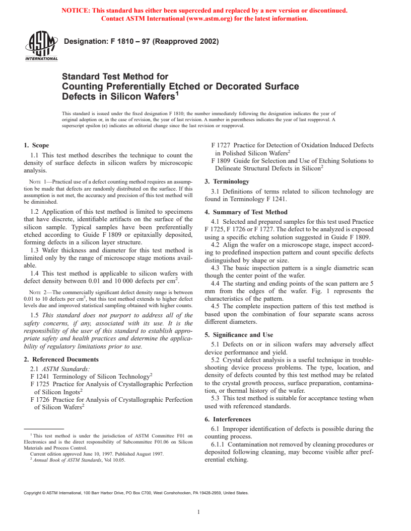
mm from the edges of the wafer. Fig. 1 represents the
NOTE 2—The commercially significant defect density range is between
0.01 to 10 defects per cm , but this test method extends to higher defect characteristics of the pattern.
levels due and improved statistical sampling obtained with higher counts.
4.5 The complete inspection pattern of this test method is
based upon the combination of four separate scans across
1.5 This standard does not purport to address all of the
different diameters.
safety concerns, if any, associated with its use. It is the
responsibility of the user of this standard to establish appro-
5. Significance and Use
priate safety and health practices and determine the applica-
5.1 Defects on or in silicon wafers may adversely affect
bility of regulatory limitations prior to use.
device performance and yield.
2. Referenced Documents
5.2 Crystal defect analysis is a useful technique in trouble-
shooting device process problems. The type, location, and
2.1 ASTM Standards:
density of defects counted by this test method may be related
F 1241 Terminology of Silicon Technology
to the crystal growth process, surface preparation, contamina-
F 1725 Practice for Analysis of Crystallographic Perfection
tion, or thermal history of the wafer.
of Silicon Ingots
5.3 This test method is suitable for acceptance testing when
F 1726 Practice for Analysis of Crystallographic Perfection
used with referenced standards.
of Silicon Wafers
6. Interferences
6.1 Improper identification of defects is possible during the
This test method is under the jurisdiction of ASTM Committee F01 on
counting process.
Electronics and is the direct responsibility of Subcommittee F01.06 on Silicon
6.1.1 Contamination not removed by cleaning procedures or
Materials and Process Control.
deposited following cleaning, may become visible after pref-
Current edition approved June 10, 1997. Published August 1997.
Annual Book of ASTM Standards, Vol 10.05. erential etching.
Copyright © ASTM International, 100 Barr Harbor Drive, PO Box C700, West Conshohocken, PA 19428-2959, United States.
NOTICE: This standard has either been superceded and replaced by a new version or discontinued.
Contact ASTM International (www.astm.org) for the latest information.
F 1810 – 97 (2002)
the field of view along the path labeled AB in Fig. 1. Points A
and B are found 5 mm from the wafer edge and the line AB is
rotated 45° from the location of the major locating flat or notch.
Alternative edge exclusion positions are acceptable with the
agreement of the parties involved.
9.1.3 Scan the path and record the classification and num-
bers of the defects observed during the scan. Refer to descrip-
tions and pictures in Guide F 1809.
9.1.4 Rotate the wafer by 45° on the microscope stage and
repeat 9.1.3 for the second scan. Refer to Fig. 2 for improved
definition of the scan pattern.
9.1.5 Rotate the wafer by 45° on the microscope stage and
repeat 9.1.3 for the third and then the fourth scans.
NOTE 1—Begin scan 5 mm from the edge.
9.2 Defect Density Calculation:
FIG. 1 The Basic Microscopic Inspection Scan Pattern
9.2.1 Count each defect class separately for each diameter
scanned. Calculate the total area inspected by multiplying four
(4) times the calibrated width of the field of view in centimeters
6.1.2 Insufficient agitation during the preferential etching
by the length of the scan in centimeters. The length (L)isthe
process may cause artifacts that may be mistaken as crystallo-
wafer diameter (D) minus twice the edge exclusion (E),
graphic defects.
6.2 The accuracy of the defect density calculation is directly
L5D2 23E!
@ ~ #
affected by calibration of the area of the microscope field of
The density is the defect count divided by the total area.
view.
NOTE 4—When a scan intersects a flat, notch or laser mark, the total
6.3 The defect density determined by this test method
area must be adjusted according to the reduced length of the affected
requires an assumption be made that defects are randomly
scans. Failure to adjust the area results in inaccuracy.
distributed on the surface. Nonuniform patterns of defects alter
the defect density measurement by their size and location.
10. Report
6.4 Multiple scan patterns intersect at the center of the
10.1 Report the following information:
wafer. If a defect is found at this single, common point, it is
10.1.1 Date of test, laboratory and operator,
counted more than once and shall alter the accuracy.
10.1.2 Identification of the specimen wafer, conductivity
type, orientation, and diameter,
7. Apparatus
10.1.3 Specimen history; thermal cycle, preferential etchant
7.1 Nonmetallic Vacuum Pickup Tool, of suitable material
formulation, thickness removal during preferential etching,
such as quartz or TFE-fluorocarbon. The pickup tool shall be
10.1.4 Inspection conditions; magnification, and total area
constructed so that no metal can contact the specimen wafer.
inspected, and
7.2 Optical Microscope, equipped with interference contrast
10.1.5 Defect density and precision by defect classification.
attachment.
11. Precision and Bias
NOTE 3—Nomarski differential interference contrast is an example of
interference contrast.
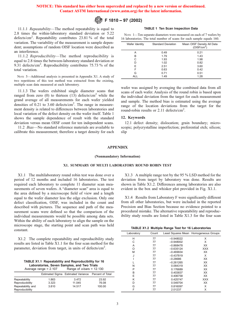
11.1 Precision—The multi laboratory precision of this test
method was established through a round-robin experiment.
7.2.1 Eyepiece and Objective Lens, in combination shall
Seven (7) wafers with randomly distributed oxidation induced
give
...


Questions, Comments and Discussion
Ask us and Technical Secretary will try to provide an answer. You can facilitate discussion about the standard in here.