Standard Test Method for Measuring Radial Resistivity Variation on Silicon Wafers

SCOPE
1.1 This test method provides procedures for the determination of relative radial variation of resistivity of semiconductor wafers cut from silicon single crystals grown either by the Czochralski or floating-zone technique.
1.2 This test method provides procedures for using Test Method F84 for the four-point probe measurement of radial resistivity variation.
1.3 This test method yields a measure of the variation in resistivity between the center and selected outer regions of the specimen. The amount of information obtained regarding the magnitude and form of the variation in the intervening regions when using the four-point probe array depends on the sampling plan chosen (see 7.2). The interpretation of the variations measured as radial variations may be in error if azimuthal variations on the wafer or axial variations along the crystal length are not negligible.
1.4 This test method can be applied to single crystals of silicon in circular wafer form, the thickness of which is less than one-half of the average probe spacing, and the diameter of which is at least 15 mm (0.6 in.). Measurements can be made on any specimen for which reliable resistivity measurements can be obtained. The resistivity measurement procedure of Test Method F84 has been tested on specimens having resistivities between 0.0008 and 2000 cm for p-type silicon and between 0.0008 and 6000 cm for n-type silicon. Geometrical correction factors required for these measurements are included for the case of standard wafer diameters, and are available in tabulated form for other cases.
Note 1--In the case of wafers whose thickness is greater than the average spacing of the measurement probes, no geometrical correction factor is available except for measurement at the center of the wafer face.
1.5 Several sampling plans are given which specify sets of measurement sites on the wafers being tested. The sampling plans allow differing levels of detail of resistivity variation to be obtained. One of these sampling plans shall be selected and agreed upon by the parties to the measurement. The basic resistivity measurements of Test Method F 84 are then applied at each site specified in the chosen sampling plan.
1.6 Results are expressed as relative changes in resistivity between the several measurement sites. To obtain absolute values of resistivity it is necessary to measure and correct for specimen temperature (see 11.1.4).
1.7 The values stated in SI units are to be regarded as the standard. The values given in parentheses are for information only.
1.8 This standard does not purport to address all of the safety concerns, if any, associated with its use. It is the responsibility of the user of this standard to establish appropriate safety and health practices and determine the applicability of regulatory limitations prior to use.

General Information

Status
Historical
Publication Date
09-Jun-2001
Technical Committee
Current Stage
Ref Project

Relations

Buy Standard

Standard
ASTM F81-00 - Standard Test Method for Measuring Radial Resistivity Variation on Silicon Wafers
English language
9 pages
sale 15% off
Preview
sale 15% off
Preview

Standards Content (Sample)


NOTICE: This standard has either been superseded and replaced by a new version or discontinued.
Contact ASTM International (www.astm.org) for the latest information.
Designation: F 81 – 00 DIN 50435
Standard Test Method for
Measuring Radial Resistivity Variation on Silicon Wafers
This standard is issued under the fixed designation F 81; the number immediately following the designation indicates the year of original
adoption or, in the case of revision, the year of last revision. A number in parentheses indicates the year of last reapproval. A superscript
epsilon (e) indicates an editorial change since the last revision or reapproval.
1. Scope 1.5 Several sampling plans are given which specify sets of
measurement sites on the wafers being tested. The sampling
1.1 This test method provides procedures for the determi-
plans allow differing levels of detail of resistivity variation to
nation of relative radial variation of resistivity of semiconduc-
be obtained. One of these sampling plans shall be selected and
tor wafers cut from silicon single crystals grown either by the
agreed upon by the parties to the measurement. The basic
Czochralski or floating-zone technique.
resistivity measurements of Test Method F 84 are then applied
1.2 This test method provides procedures for using Test
at each site specified in the chosen sampling plan.
Method F 84 for the four-point probe measurement of radial
1.6 Results are expressed as relative changes in resistivity
resistivity variation.
between the several measurement sites. To obtain absolute
1.3 This test method yields a measure of the variation in
values of resistivity it is necessary to measure and correct for
resistivity between the center and selected outer regions of the
specimen temperature (see 11.1.4).
specimen. The amount of information obtained regarding the
1.7 The values stated in SI units are to be regarded as the
magnitude and form of the variation in the intervening regions
standard. The values given in parentheses are for information
when using the four-point probe array depends on the sampling
only.
plan chosen (see 7.2). The interpretation of the variations
1.8 This standard does not purport to address all of the
measured as radial variations may be in error if azimuthal
safety concerns, if any, associated with its use. It is the
variations on the wafer or axial variations along the crystal
responsibility of the user of this standard to establish appro-
length are not negligible.
priate safety and health practices and determine the applica-
1.4 This test method can be applied to single crystals of
bility of regulatory limitations prior to use.
silicon in circular wafer form, the thickness of which is less
than one-half of the average probe spacing, and the diameter of
2. Referenced Documents
which is at least 15 mm (0.6 in.). Measurements can be made
2.1 ASTM Standards:
on any specimen for which reliable resistivity measurements
F 84 Test Methods for Measuring Resistivity of Silicon
can be obtained. The resistivity measurement procedure of Test
Wafers with an In-Line Four-Point Probe
Method F 84 has been tested on specimens having resistivities
2.2 SEMI Standard:
between 0.0008 and 2000 V·cm for p-type silicon and between
Specifications M 1, S for Polished Monocrystalline Silicon
0.0008 and 6000 V·cm for n-type silicon. Geometrical correc-
Wafers
tion factors required for these measurements are included for
the case of standard wafer diameters, and are available in
3. Summary of Test Method
tabulated form for other cases.
3.1 Resistivity measurements are made at specified sites
NOTE 1—In the case of wafers whose thickness is greater than the
along one or two diameters of a semiconductor specimen in
average spacing of the measurement probes, no geometrical correction
accordance with a sampling plan selected from the four given.
factor is available except for measurement at the center of the wafer face.
Choice among the sampling plans is made on the basis of the
extent of information required regarding possible resistivity
variations. The measured resistivity values are corrected for
This test method is under the jurisdiction of ASTM Committee F1 on
specimen geometry and, if desired, for temperature, and
Electronics, and is the direct responsibility of Subcommittee F01.06 on Silicon
suitable differences are taken to obtain the resistivity variation.
Materials and Process Control.
Current edition approved Dec. 10, 2000. Published February 2001. Originally
4. Significance and Use
published as F 81 – 67 T. Last previous edition F 81 – 95.
DIN 50435 is an equivalent method. It is the responsibility of DIN Committee
4.1 The radial resistivity variation of bulk semiconductor
NMP 221, with which Committee F-1 maintains close liaison. DIN 50435,
material is an important materials acceptance requirement for
Determination of the Radial Resistivity Variation of Silicon or Germanium Slices by
Means of a Four-Point DC-Probe, is available from Beuth Verlag GmbH, Burg-
grafenstrasse 4-10, D-1000 Berlin 30,
Swartzendruber, L. J., “Correction Factor Tables for Four-Point Probe Resis-
tivity Measurements on Thin Circular Semiconductor Samples,” Technical Note Annual Book of ASTM Standards, Vol 10.05.
199, NBTNA, National Bureau of Standards, April 15, 1964. Available as AD 683 Available from Semiconductor Equipment and Materials International, 805
408 from National Technical Information Service, Springfield, Va. 22161. East Middlefield Road, Mountain View, CA 94043.
Copyright © ASTM, 100 Barr Harbor Drive, West Conshohocken, PA 19428-2959, United States.
F81
semiconductor device fabrication and is also used for quality proximity to an orientation flat on a wafer, or if the wafer
control purposes. surfaces are conducting.
4.2 The four-point probe method provides a test that re- 5.4.2 Additional errors in the correction factor are encoun-
quires little specimen preparation and that is nondestructive in tered if the true wafer diameter is not used in calculating the
that the wafer is left intact. The method can be applied to correction factor. Use of the nominal diameter for all wafers of
wafers using the resistivity-measuring apparatus and proce- standard dimensions with diametral tolerances allowed by
dures of Test Method F 84 if provisions are made for making SEMI Specifications M 1 introduces negligible error if mea-
measurements at several sites on the wafer (see 6.1). Appro- surements are made no closer to the edge of the wafer than 6
priate correction factors must be applied to compensate for mm. Appendix X2 gives magnitudes of the error in the
effects of the wafer geometry (see 11.1). geometrical correction factor and in the resulting local resis-
4.3 Radial resistivity variations are a function of the crystal tivity values which result when the nominal wafer diameter is
growth process and dopant, both in characteristic shape and used in the calculation for specimen which have the smallest
magnitude. Because no single sampling plan is adequate to diameter allowed by SEMI Specifications M 1.
characterize the resistivity variations of all crystal types or for 5.4.3 The wafer thickness enters directly into the calculation
all applications, four sampling plans are included in this test of resistivity from the measured voltage-to-current ratio. Ap-
method. pendix X2 gives magnitudes of the error in the local resistivity
values when the nominal wafer thickness is used in the
5. Interferences
calculation for wafers with the smallest center-point thickness
5.1 Current Level— The current levels as a function of
allowed by SEMI Specification M 1 and a local thickness that
resistivity recommended in Test Method F 84 have been found
deviates from the nominal value by ( 1) the maximum allowed
satisfactory for the specified probe spacing and specimen size
by SEMI Specifications M 1 or (2) the 13 μm (0.0005 in.)
range. However, should smaller than recommended probe
allowed by Test Method F 84. If more accurate determinations
spacing be used, or very long lifetime specimens be measured,
of local resistivity are required, (1) the thickness at each
the suitability of the recommended currents should be estab-
measurement site should be determined and used in calculating
lished by doubling and halving the recommended current and
the resistivity at that site, (2) wafers with smaller thickness
checking for a resulting doubling and halving of measured
variation should be employed, or (3) thicker wafers should be
specimen voltage. It is then recommended that a current near
employed.
the middle of the range giving a constant measure of resistivity
5.5 Polished Surfaces—Measurements on a polished rather
be used.
than a lapped wafer surface as required in this method will in
5.2 Longitudinal Resistivity Variations—The local fluctua-
general give satisfactory measurement results. However, the
tions in dopant density which cause resistivity variations on a
possibility of measurement errors due to surface conduction or
cross section of a semiconductor crystal also cause axial
to low surface recombination velocity requires the use of
resistivity variations down the length of the crystal. The
lapped wafer surfaces for referee measurements.
four-point probe method measures averaged local resistivity
5.6 Temperature fluctuations of specimen temperature dur-
values, and these averaged values are influenced by resistivity
ing the measurement time will affect the measurement. This
changes through the thickness of the specimens. The extent of
can be corrected if the specimen temperature is known (see
this influence depends on probe spacing. Radial variation
11.1.4 and Note 4).
measurements on the front and back sides of a wafer may differ
6. Apparatus
because of longitudinal variations.
5.3 Accuracy of Probe Placement—The position of the 6.1 Apparatus as specified in Test Method F 84 is required
probe head may have a noticeable effect on the measured for four-point probe measurement, except that the specimen
voltage-to-current ratio because of the proximity of the probe support shall include an x-y stage with micrometer adjustment
tips to a wafer boundary. Geometrical correction factors used capable of positioning the probe head at specified points on the
to calculate the local resistivity from the measured voltage and specimen with an accuracy of 60.15 mm; it shall also include
current values are calculated for a particular position of the provision for rotating the specimen through 360° with a
probe head with respect to the wafer center and wafer rotational accuracy of 65°.
boundaries. Appendix X1 gives magnitudes of the error in the
7. Sampling
geometrical correction factor and in resulting local resistivity
7.1 The sampling plan for selection of wafers from a lot
values if the position of a probe with a 1.59-mm probe tip
shall be agreed upon by the parties to the measurement.
spacing shifted the maximum allowed value, 0.15 mm (0.006
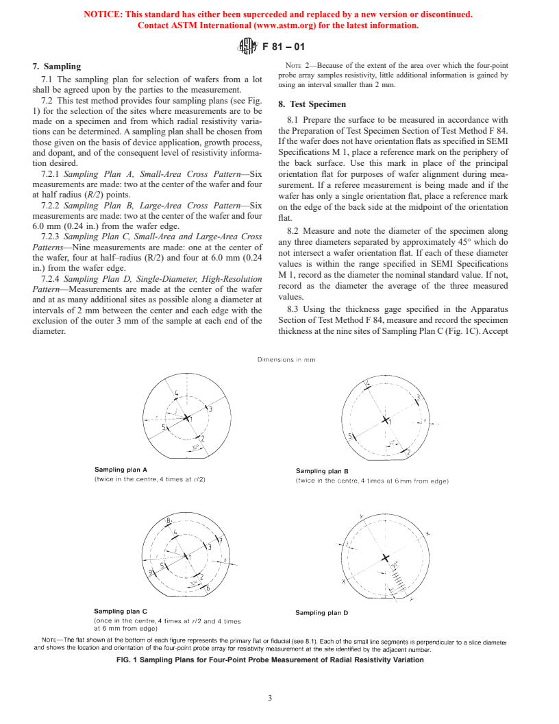
7.2 This test method provides four sampling plans (see Fig.
in.), toward the edge of the wafer. These errors decrease with
1) for the selection of the sites where measurements are to be
decreasing probe spacing for all wafer sizes and measurement
sites.
5.4 Wafer-Geometry Related Errors: 6
Ehrstein, J. R., Brewer, F. H., Ricks, D. R., and Bullis, W. M.,“ Effects of
5.4.1 The geometrical correction factors used to calculate
Current, Probe, Force and Wafer Surface Condition on Measurement of Resistivity
of Bulk Silicon Wafers by the Four-Probe Method,” Appendix E, “Methods of
the local resistivity from the measured voltage and current
Measurement for Semiconductor Materials, Process Control, and Devices,” Tech-
ratios depend on the assumptions of full circular wafer geom-
nical Note 773, NBTNA, National Bureau of Standards, June 1973, pp. 43–49.
etry and of nonconducting wafer back side and edges. As a
Available as COM 73-50534 from National Technical Information Service, Spring-
result, some error is introduced if measurements are made in field, Va. 22161.
F81
FIG. 1 Sampling Plans for Four-Point Probe Measurement of Radial Resistivity Variation
made on a specimen and from which radial resistivity varia- If the wafer does not have orientation flats as specified in SEMI
tions can be determined. A sampling plan shall be chosen from Specifications M 1, place a reference mark on the periphery of
those given on the basis of device application, growth process, the back surface. Use this mark in place of the principal
and dopant, and of the consequent level of resistivity informa- orientation flat for purposes of wafer alignment during mea-
tion desired. surement. If a referee measurement is being made and if the
7.2.1 Sampling Plan A, Small-Area Cross Pattern—Six wafer has only a single orientation flat, place a reference mark
measurements are made: two at the center of the wafer and four on the edge of the back side at the midpoint of the orientation
at half radius (R/2) points. flat.
7.2.2 Sampling Plan B, Large-Area Cross Pattern—Six 8.2 Measure and note the diameter of the specimen along
measurements are made: two at the center of the wafer and four any three diameters separated by approximately 45° which do
6.0 mm (0.24 in.) from the wafer edge. not intersect a wafer orientation flat. If each of these diameter
7.2.3 Sampling Plan C, Small-Area and Large-Area Cross values is within the range specified in SEMI Specifications
Patterns—Nine measurements are made: one at the center of M 1, record as the diameter the nominal standard value. If not,
the wafer, four at half–radius (R/2) and four at 6.0 mm (0.24 record as the diameter the average of the three measured
in.) from the wafer edge. values.
7.2.4 Sampling Plan D, Single-Diameter, High-Resolution 8.3 Using the thickness gage specified in the Apparatus
Pattern—Measurements are made at the center of the wafer Section of Test Method F 84, measure and record the specimen
and at as many additional sites as possible along a diameter at thickness at the nine sites of Sampling Plan C (Fig. 1C). Accept
intervals of 2 mm between the center and each edge with the a specimen for measurement if the total thickness variation is
exclusion of the outer 3 mm of the sample at each end of the less than 13 μm (0.0005 in.) (see 5.4.3).
diameter.
9. Suitability of Test Equipment
NOTE 2—Because of the extent of the area over which the four-point
9.1 Determine the suitability of the four-point probe and
probe array samples resistivity, little additional information is gained by
electronics for use in measuring resistivity in accordance with
using an interval smaller than 2 mm.
the Suitability of Test Equipment Section of Test Method F 84.
8. Test Specimen
10. Procedure
8.1 Prepare the surface to be measured in accordance with
the Preparation of Test Specimen Section of Test Method F 84. 10.1 Align the specimen so that the first measurement
...

Questions, Comments and Discussion

Ask us and Technical Secretary will try to provide an answer. You can facilitate discussion about the standard in here.