

IEC PAS 63720:2026
(Main)Rigid circuit board - Routing parameters
- Abstract
IEC PAS 63720:2026 defines standardized routing parameter tables applicable to the design of rigid circuit board with mechanically or laser drilled vias.
These parameter tables are based on the concept of "Routing Classes" initially introduced in the French standard NF-93713 (1971-1989, cancelled: 2019). They are linked to the pitch of electronic components (e.g., BGA, QFN, connector, etc.) and thus allow a better coupling with component and circuit board manufacturers.
They can be easily integrated into EDA tools to facilitate the work of designers, while ensuring a common standard of communication between customers and manufacturers.
Routing classes should not be confused with IPC performance classes, which are used in the context of circuit board acceptance (IPC-A-600) as well as qualification and performance (IPC-6012) standards. Additional information on circuit board design is provided by IPC-2221 (Generic Standard on Printed Board Design), IPC-2222 (Sectional Design Standard for Rigid Organic Printed Boards) and IPC-2226 (Sectional Design Standard for High Density Interconnect (HDI) Printed Boards).
This document is based on French AFNOR Spec 2212 and was submitted as a PAS document.
- Status
- Published
- Publication Date
- 05-Aug-2026
- Technical Committee
- TC 91 - Electronics assembly technology
- Drafting Committee
- WG 12 - TC 91/WG 12
- Current Stage
- PPUB - Publication issued
- Start Date
- 06-Aug-2026
- Completion Date
- 04-Sep-2026

IEC PAS 63720:2026 is an IEC Publicly Available Specification from the International Electrotechnical Commission for rigid circuit board routing parameters. It specifies standardized routing parameter tables for rigid printed board design with mechanically or laser-drilled vias, so designers, manufacturers and buyers can use the same class system for conductor widths, spacings, drilling, solder mask and marking.
What does IEC PAS 63720:2026 specify?
IEC PAS 63720:2026 defines routing parameter tables for designing rigid circuit boards with mechanically or laser-drilled vias. The document links those tables to component pitch and board structure, so the chosen routing class can be matched to the package and to manufacturing capability.
The document is organized into these clauses:
- Clause 1 - Scope
- Clause 2 - Definitions and conventions
- Clause 3 - Component packages and printed board structure
- Clause 4 - Mechanical parameters
- Clause 5 - Conductor parameters
- Clause 6 - Drilling parameters for plated-through holes and mechanically drilled vias
- Clause 7 - Drilling parameters for laser-drilled microvias
- Clause 8 - Solder mask parameters
- Clause 9 - Ink marking parameters
A key point in practice is that Routing Classes are design rules, not inspection or acceptance classes. The standard also notes that panelization is not covered, and that routing classes should not be confused with IPC performance classes used for acceptance, qualification and performance.
What are the key requirements of IEC PAS 63720:2026?
Routing classes and how to choose them
IEC PAS 63720:2026 defines Routing Classes (RC) from RC1 to RC10 as sets of compatible design parameters. Higher classes allow denser routing, but they also increase manufacturing difficulty and can raise cost or make production impractical.
Clause 3 ties the class choice to component package pitch, such as BGA, QFN, connectors and discrete SMD parts. In practice, the designer starts from the component package and the required interconnect density, then selects the lowest class that still allows the routing. When several RCs are used on one board, the highest RC used anywhere defines the board’s RC.
Parameter system and value conventions
Clause 2 splits the parameters into six sections: ME, CO, VM/TM, UV, SM and MA. Uppercase identifiers indicate values, while lowercase identifiers indicate tolerances. This matters because the tables distinguish the nominal design value from the allowed variation.
The document also gives a strict reading for table entries: the first value is preferred, a value in brackets is a limit that should not be exceeded, square brackets indicate a selectable range, and N/A means a non-recommended configuration. That helps teams decide whether a layout is preferred, acceptable only as a limit, or not suited to the class.
Mechanical limits for outline, spacing and thickness
Clause 4 covers mechanical parameters such as board length and width, cutting radius, distances from board edges, V-scoring and non-plated-through holes, and maximum stack-up thickness. It also gives tolerances for routing, hole spacing, hole diameters and finished thickness.
In practice, these tables are used when checking whether the outline, cutouts, hole placement and board thickness fit the selected class. The clause also makes it clear that plated board outlines add constraints outside the scope of the document, and that printed circuit panelization is not covered.
Conductor widths, spacings and copper thickness
Clause 5 sets the conductor rules for minimum width, spacing between tracks, spacing to planes, spacing around via pads, and finished copper thickness on plated and non-plated layers. It also distinguishes NSMD and SMD pad spacing, which matters because pad style changes the available copper-clearance geometry.
The conductor tables allow different RCs on different layers, but the highest class used anywhere still defines the board class. For manufacturing, this means the copper thickness, plating process and layer balance must be coordinated early, especially for high-density routing and plated structures.
Drilling rules for plated-through holes and mechanically drilled vias
Clause 6 defines drilling parameters for mechanically drilled holes and plated-through holes. It includes minimum drilled hole diameter as a function of the thickness to be drilled, minimum via pad diameter by drilled hole size, and pad diameters for plated-through holes used for component insertion by soldering.
This clause is where drill size, stack-up thickness and pad size have to line up. The document also notes that the annular ring after manufacture is the responsibility of the PCB manufacturer, so the designer has to specify the intent clearly and the fabricator has to achieve it.
Laser-drilled microvias, solder mask and ink marking
Clause 7 sets the microvia rules and states that using a microvia requires a routing class of RC6 or higher. It also links microvia pad diameter, drilling diameter and dielectric thickness, and it gives minimum spacing rules for microvias on the same potential and between microvia and mechanical via pads.
Clause 8 covers solder mask distance to soldered pads, minimum solder mask dam, minimum opening, opening tolerance and spacing to routing or hole edges. Clause 9 then covers ink marking on solder mask, and says copper marking is preferred but limited to RC6. In practice, these clauses control whether the board can be assembled cleanly and whether marking can be placed without disturbing copper or solder mask features.
What terms does IEC PAS 63720:2026 define?
- Routing Classes (RC) - design rules that group compatible routing parameters for a given PCB manufacturing difficulty.
- BGA (Ball Grid Array) - a surface-mount package with balls arranged in a grid on the underside.
- QFN (Quad Flat No-lead) - a rectangular package whose terminals end on the package base edges.
- NSMD (Non-Solder Mask Defined) - a pad style where the solder mask opening is larger than the copper pad.
- SMD (Solder Mask Defined) - a pad style where the solder mask opening is smaller than the copper pad.
- Plated-Through Hole (PTH) - a hole plated on its walls to connect conductive patterns on different layers.
- Microvia - a blind via with a maximum aspect ratio of 1:1 and a total depth of no more than 0.25 mm.
- Pitch - the nominal center-to-center distance between adjacent equal-size features.
Who uses IEC PAS 63720:2026?
IEC PAS 63720:2026 is used by PCB designers, board fabricators, assembly engineers, component suppliers and quality or procurement teams who need a common routing language. It is especially relevant when selecting routing rules for BGA, QFN, connectors and other SMD packages, or when agreeing drill, copper, solder mask and marking constraints with a manufacturer.
It also helps EDA tool users and tool integrators because the parameter tables can be built into design-rule checks and data packages. For buyers and quality managers, the class system gives a practical way to compare manufacturability across suppliers without treating routing class as a product acceptance grade.
Which standards are used with IEC PAS 63720:2026?
- IPC-A-600 - used as the acceptance context where IPC performance classes apply, which are different from Routing Classes.
- IPC-6012 - used for qualification and performance context for circuit boards.
- IPC-2221 - provides generic printed board design guidance alongside this document.
- IPC-2222 - provides sectional design guidance for rigid organic printed boards.
- IPC-2226 - provides sectional design guidance for HDI printed boards.
- IPC-T-50M EN - supplies several of the package, via and process definitions cited in Clause 2.
What does the IEC PAS 63720:2026 document contain?
The document contains the routing class concept, the conventions for reading values and tolerances, and detailed parameter tables for each class. It also includes figures that illustrate board structures, drilling geometry, solder mask geometry and marking geometry.
Tables 2 and 3 link RC selection to component package pitch and via or board structure, which is the practical starting point for design. Tables 4 to 11 then give the numeric values and tolerances for mechanical features, conductors, plated and laser-drilled vias, solder mask and ink marking.
The document is intended for design definition, supplier communication and manufacturability checks. Its content is structured so it can be translated into layout rules, fabrication constraints and automated checks in design tools.
Frequently Asked Questions
IEC PAS 63720:2026 is a technical specification published by the International Electrotechnical Commission (IEC). Its full title is "Rigid circuit board - Routing parameters". This standard covers: IEC PAS 63720:2026 defines standardized routing parameter tables applicable to the design of rigid circuit board with mechanically or laser drilled vias. These parameter tables are based on the concept of "Routing Classes" initially introduced in the French standard NF-93713 (1971-1989, cancelled: 2019). They are linked to the pitch of electronic components (e.g., BGA, QFN, connector, etc.) and thus allow a better coupling with component and circuit board manufacturers. They can be easily integrated into EDA tools to facilitate the work of designers, while ensuring a common standard of communication between customers and manufacturers. Routing classes should not be confused with IPC performance classes, which are used in the context of circuit board acceptance (IPC-A-600) as well as qualification and performance (IPC-6012) standards. Additional information on circuit board design is provided by IPC-2221 (Generic Standard on Printed Board Design), IPC-2222 (Sectional Design Standard for Rigid Organic Printed Boards) and IPC-2226 (Sectional Design Standard for High Density Interconnect (HDI) Printed Boards). This document is based on French AFNOR Spec 2212 and was submitted as a PAS document.
IEC PAS 63720:2026 defines standardized routing parameter tables applicable to the design of rigid circuit board with mechanically or laser drilled vias. These parameter tables are based on the concept of "Routing Classes" initially introduced in the French standard NF-93713 (1971-1989, cancelled: 2019). They are linked to the pitch of electronic components (e.g., BGA, QFN, connector, etc.) and thus allow a better coupling with component and circuit board manufacturers. They can be easily integrated into EDA tools to facilitate the work of designers, while ensuring a common standard of communication between customers and manufacturers. Routing classes should not be confused with IPC performance classes, which are used in the context of circuit board acceptance (IPC-A-600) as well as qualification and performance (IPC-6012) standards. Additional information on circuit board design is provided by IPC-2221 (Generic Standard on Printed Board Design), IPC-2222 (Sectional Design Standard for Rigid Organic Printed Boards) and IPC-2226 (Sectional Design Standard for High Density Interconnect (HDI) Printed Boards). This document is based on French AFNOR Spec 2212 and was submitted as a PAS document.
IEC PAS 63720:2026 is classified under the following ICS (International Classification for Standards) categories: 31.180 - Printed circuits and boards; 31.190 - Electronic component assemblies. The ICS classification helps identify the subject area and facilitates finding related standards.
IEC PAS 63720:2026 is available in PDF format for immediate download after purchase. The document can be added to your cart and obtained through the secure checkout process. Digital delivery ensures instant access to the complete standard document.
Standards Content (Sample)
IEC PAS 63720 ®
Edition 1.0 2026-08
PUBLICLY AVAILABLE
SPECIFICATION
Rigid circuit board - Routing parameters
ICS 31.180; 31.190 ISBN 978-2-8327-1426-3
All rights reserved. Unless otherwise specified, no part of this publication may be reproduced or utilized in any form or
by any means, electronic or mechanical, including photocopying and microfilm, without permission in writing from either
IEC or IEC's member National Committee in the country of the requester. If you have any questions about IEC copyright
or have an enquiry about obtaining additional rights to this publication, please contact the address below or your local
IEC member National Committee for further information.
IEC Secretariat Tel.: +41 22 919 02 11
3, rue de Varembé info@iec.ch
CH-1211 Geneva 20 www.iec.ch
Switzerland
About the IEC
The International Electrotechnical Commission (IEC) is the leading global organization that prepares and publishes
International Standards for all electrical, electronic and related technologies.
About IEC publications
The technical content of IEC publications is kept under constant review by the IEC. Please make sure that you have the
latest edition, a corrigendum or an amendment might have been published.
IEC publications search - IEC Products & Services Portal - products.iec.ch
webstore.iec.ch/advsearchform Discover our powerful search engine and read freely all the
The advanced search enables to find IEC publications by a
publications previews, graphical symbols and the glossary.
variety of criteria (reference number, text, technical With a subscription you will always have access to up to date
committee, …). It also gives information on projects, content tailored to your needs.
replaced and withdrawn publications.
Electropedia - www.electropedia.org
IEC Just Published - webstore.iec.ch/justpublished The world's leading online dictionary on electrotechnology,
Stay up to date on all new IEC publications. Just Published containing more than 22 500 terminological entries in English
details all new publications released. Available online and and French, with equivalent terms in 25 additional languages.
once a month by email. Also known as the International Electrotechnical Vocabulary
(IEV) online.
IEC Customer Service Centre - webstore.iec.ch/csc
If you wish to give us your feedback on this publication or
need further assistance, please contact the Customer
Service Centre: sales@iec.ch.
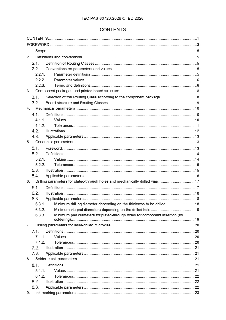
CONTENTS
CONTENTS . 1
FOREWORD . 3
1. Scope . 5
2. Definitions and conventions. 5
Definition of Routing Classes . 5
Conventions on parameters and values . 5
2.2.1. Parameter definitions . 5
2.2.2. Parameter values . 6
2.2.3. Terms and definitions . 6
3. Component packages and printed board structure . 8
Selection of the Routing Class according to the component package . 8
Board structure and Routing Classes . 9
4. Mechanical parameters . 10
Definitions . 10
4.1.1. Values . 10
4.1.2. Tolerances . 11
Illustrations . 12
Applicable parameters . 13
5. Conductor parameters. 13
Foreword . 13
Definitions . 14
5.2.1. Values . 14
5.2.2. Tolerances . 15
Illustration . 15
Applicable parameters . 16
6. Drilling parameters for plated-through holes and mechanically drilled vias . 17
Definitions . 17
Illustration . 18
Applicable parameters . 18
6.3.1. Minimum drilling diameter depending on the thickness to be drilled . 18
6.3.2. Minimum via pad diameters depending on the drilled hole . 19
6.3.3. Minimum pad diameters for plated-through holes for component insertion (by
soldering) . 19
7. Drilling parameters for laser-drilled microvias . 20
Definitions . 20
7.1.1. Values . 20
7.1.2. Tolerances . 20
Illustration . 21
Applicable parameters . 21
8. Solder mask parameters . 21
Definitions . 21
8.1.1. Values . 21
8.1.2. Tolerances . 22
Illustration . 22
Applicable parameters . 22
9. Ink marking parameters. 23
Definition . 23
Illustration . 24
Applicable parameters . 24
INTERNATIONAL ELECTROTECHNICAL COMMISSION
____________
Rigid circuit board - Routing parameters
FOREWORD
1) The International Electrotechnical Commission (IEC) is a worldwide organization for standardization comprising
all national electrotechnical committees (IEC National Committees). The object of IEC is to promote international
co-operation on all questions concerning standardization in the electrical and electronic fields. To this end and
in addition to other activities, IEC publishes International Standards, Technical Specifications, Technical Reports,
Publicly Available Specifications (PAS) and Guides (hereafter referred to as "IEC Publication(s)"). Their
preparation is entrusted to technical committees; any IEC National Committee interested in the subject dealt with
may participate in this preparatory work. International, governmental and non-governmental organizations liaising
with the IEC also participate in this preparation. IEC collaborates closely with the International Organization for
Standardization (ISO) in accordance with conditions determined by agreement between the two organizations.
2) The formal decisions or agreements of IEC on technical matters express, as nearly as possible, an international
consensus of opinion on the relevant subjects since each technical committee has representation from all
interested IEC National Committees.
3) IEC Publications have the form of recommendations for international use and are accepted by IEC National
Committees in that sense. While all reasonable efforts are made to ensure that the technical content of IEC
Publications is accurate, IEC cannot be held responsible for the way in which they are used or for any
misinterpretation by any end user.
4) In order to promote international uniformity, IEC National Committees undertake to apply IEC Publications
transparently to the maximum extent possible in their national and regional publications. Any divergence between
any IEC Publication and the corresponding national or regional publication shall be clearly indicated in the latter.
5) IEC itself does not provide any attestation of conformity. Independent certification bodies provide conformity
assessment services and, in some areas, access to IEC marks of conformity. IEC is not responsible for any
services carried out by independent certification bodies.
6) All users should ensure that they have the latest edition of this publication.
7) No liability shall attach to IEC or its directors, employees, servants or agents including individual experts and
members of its technical committees and IEC National Committees for any personal injury, property damage or
other damage of any nature whatsoever, whether direct or indirect, or for costs (including legal fees) and
expenses arising out of the publication, use of, or reliance upon, this IEC Publication or any other IEC
Publications.
8) Attention is drawn to the Normative references cited in this publication. Use of the referenced publications is
indispensable for the correct application of this publication.
9) IEC draws attention to the possibility that the implementation of this document may involve the use of (a)
patent(s). IEC takes no position concerning the evidence, validity or applicability of any claimed patent rights in
respect thereof. As of the date of publication of this document. IEC had not received notice of a patent, which
may be required to implement this document. However, implementers are cautioned that this may not represent
the latest information, which may be obtained from the patent database available at https://patents.iec.ch. IEC
shall not be held responsible for identifying any or all such patent rights.
IEC PAS 63720 has been prepared by IEC technical committee 91: Electronics assembly
technology. It is a Publicly Available Specification.
It is based on French AFNOR Spec 2212 and was submitted as a PAS document.
The text of this Publicly Available Specification is based on the following documents:
Draft Report on voting
91/2112/DPAS 91/2123/RVDPAS
Full information on the voting for its approval can be found in the report on voting indicated in
the above table.
The language used for the development of this Publicly Available Specification is English.
The structure and editorial rules used in this publication reflect the practice of the organization
which submitted it.
This document was developed in accordance with ISO/IEC Directives, Part 1 and ISO/IEC
Directives, IEC Supplement, available at www.iec.ch/members_experts/refdocs. The main
document types developed by IEC are described in greater detail at www.iec.ch/publications.
The committee has decided that the contents of this document will remain unchanged until the
stability date indicated on the IEC website under webstore.iec.ch in the data related to the
specific document. At this date, the document will be
– reconfirmed,
– withdrawn, or
– revised.
NOTE In accordance with ISO/IEC Directives, Part 1, IEC PASs are automatically withdrawn after 4 years.
1. Scope
This document defines standardized routing parameter tables applicable to the design of rigid circuit
board with mechanically or laser drilled vias.
These parameter tables are based on the concept of "Routing Classes" initially introduced in the French
standard NF-93713 (1971-1989, cancelled: 2019). They are linked to the pitch of electronic components
(e.g., BGA, QFN, connector, etc.) and thus allow a better coupling with component and circuit board
manufacturers.
They can be easily integrated into EDA tools to facilitate the work of designers, while ensuring a common
standard of communication between customers and manufacturers.
Routing classes should not be confused with IPC performance classes, which are used in the context
of circuit board acceptance (IPC-A-600) as well as qualification and performance (IPC-6012) standards.
Additional information on circuit board design is provided by IPC-2221 (Generic Standard on Printed
Board Design), IPC-2222 (Sectional Design Standard for Rigid Organic Printed Boards) and IPC-2226
(Sectional Design Standard for High Density Interconnect (HDI) Printed Boards).
2. Definitions and conventions
Definition of Routing Classes
Routing Classes (RC) are design rules for routing printed boards. This concept is based on the previous
NF C93-713 standard.
Each Routing Class, from RC1 to RC10 corresponds to a set of parameters that are compatible with a
given type of component package and consistent in terms of PCB manufacturing difficulty. A higher RC
allows for a greater level of component density, but implies a higher degree of manufacturing difficulty,
which increases costs, it can even makes production impossible. Classes RC1 and RC2 should only be
used for designs which contain conductors with high copper thicknesses
Class RC10 is given prospectively. Organic substrates for semiconductors or SiP (system in package)
requiring conductor widths/spacings above Class 10 are not covered in this document.
Routing Classes are not inspection criteria or quality requirements for the delivered product and
should therefore not be confused with control classes. Each user and manufacturer is
responsible for identifying the applicable Routing Classes according to the expected quality and
performance requirements for the end product.
Conventions on parameters and values
2.2.1. Parameter definitions
Routing Class parameters are divided into six main sections and identified by two letters. Uppercase
characters indicate a value, while lowercase characters specify a tolerance.
Table 1 - Parameters and conventions
Value Tolerance Section parameters
ME me MEchanical
CO co COnductors
VM (TM) vm (tm) Vias (Holes) - Mechanically drilled
UV uv UVia (microvia)
SM sm Solder Mask
MA ma MArking
Note: for each section, the parameters are identified by two letters and a number. For example, CO4 means
conductor parameter no. 4, while me13 means mechanical parameter no. 13 and represents a tolerance.
2.2.2. Parameter values
Values are associated in the tables for each parameter/Routing Class using the following conventions:
The first value, shown, is the preferred value.
An additional value in brackets, indicates a limit value that should not be exceeded and whose use
should be restricted as far as possible.
Values in square brackets, indicate the possibility of choosing from the specified range of values.
N/A (not applicable) or no value, means a non-recommended configuration.
2.2.3. Terms and definitions
2.2.3.1. Components
QFP (Quad Flat Package)* Pressfit Contact*
A generic rectangular component package, An electrical contact that can be pressed into a
containing an electronic device, with surface hole in an insulator or printed board with or
mount terminals on all four sides. without plated-through holes.
QFN (Quad Flat No-lead)* NSMD (Non-Solder Mask Defined)
A generic rectangular component package, The solder mask opening is larger than the
whose contours are terminated by metal lands
copper pads of the component's footprint.
on all four sides of the package base.
BGA (Ball Grid Array)* SMD (Solder Mask Defined)
A surface mount package, wherein the balls for The solder mask opening is smaller than the
terminations are formed in a grid, on the copper pads of the component's footprint.
underside of the package.
SMD (Surface-Mount Device)* Pitch*
A leaded or leadless device (part) that is The nominal center-to-center distance of
adjacent features (when the elements are of
capable of being attached to a printed board by
surface mounting. equal size and their spacing is uniform).
* Source: IPC-T-50M EN
2.2.3.2. Drilling and vias
Microvia*
Blind via*
A blind structure (as plated) with a maximum
A via that connects an outer layer to one or more
aspect ratio of 1:1 and terminating on, or
inner layers, but does not go through the entire
penetrating a target land, with a total depth (X)
printed board.
of no more than 0.25 mm [0.00984 in]. It is
measured from the structure's capture land foil
Buried via*
to the target land.
A via that does not extend to the surface of a
printed board.
Microvia/Via-in-pad
Mechanical via
Microvia or via with capture pad, within a
components copper pad.
A via drilled with a drill bit on mechanical drilling
equipment.
Aspect Ratio (Hole)*
Stacked via (microvia)*
The ratio of the length, or depth, of a hole to its
preplated diameter.
A structure formed by vertically aligning
vias/microvias, directly on top of each other (or
on top of a buried via).
Plated-Through Hole (PTH)*
Filled via*
A hole with plating on its walls, that makes an
electrical connection between conductive
A via filled with material applied into the via
patterns on internal layers, external layers, or
targeting full penetration and encapsulation of
both, of a printed board.
the hole.
Filled and capped via*
Via*
A plated structure formed by mechanical, laser A filled via with a secondary metallized coating
covering the via. The metallization is on both
or photo-defined means that is used as an
interlayer connection but is not intended for sides.
inserting a component lead or metallic part.
* Source: IPC-T-50M EN
2.2.3.3. End product and other processes
Sequentially-Laminated Multilayer Printed Hot Air (Solder) Leveling (HASL)
Board*
A physical deposition process using a solder
A multilayer printed board that is formed by bath, into which the printed board is immersed
laminating together, through-hole, plated in a bath of molten solder and withdrawn across
double-sided or multilayer boards. (Thus, some a set of hot air knives (forced hot air flow) to
of its conductive layers are interconnected with remove excess solder.
blind or buried vias).
Routing (milling)* V-Scoring*
A mechanical method that removes a portion of The machining of a shallow, precise V-shaped
the material outlining a printed board, using a groove into the top and bottom surfaces of the
cutting bit, in order to facilitate ease of breakout, laminate, in a straight line, in order to facilitate
(removal) from the manufacturing or assembly ease of breakout, (removal) from the
manufacturing or assembly panel.
panel.
Finished copper thickness End Product*
The finished copper thickness takes account of An individual part or assembly, in its final
the initial copper thickness (base copper), the completed state.
thickness after one or more copper platings and
thickness reductions due to the various
manufacturing processes.
* Source: IPC-T-50M EN
3. Component packages and printed board structure
Selection of the Routing Class according to the component
package
The conductor dimensions and spacings and therefore the Routing Classes (RC) to be used, are closely
linked to the layout and pitch of the package's lead pins.
The following tables show which RC should be used, depending on the type of package chosen and the
associated routing requirements. Other functional criteria may lead to a different routing class to the
recommended RC.
Wherever possible, use the lowest RC and limit the use of higher classes for local component routing.
When several RC are used for the same board, the highest RC (even used locally) defines the board's
RC and therefore its price.
The boxes marked with a tick () represent the recommended RC for the components mentioned. A
higher RC may be required in certain situations, such as the need to route two conductors between vias.
In addition, a lower RC may also be used if routing requirements are lower.
Table 2 - Preferred Routing Classes (RC) by component type
Routing Classes
Pitch
Component types
RC1-
(mm)
RC4 RC5 RC6 RC7 RC8 RC9 RC10
2,54
1,27
1,0
0,8
Matrix components (BGA or
similar)
0,65
0,5
0,4
0,3
> 0,5
SMC: QFP, QFN,
connectors, discrete 0,5
...