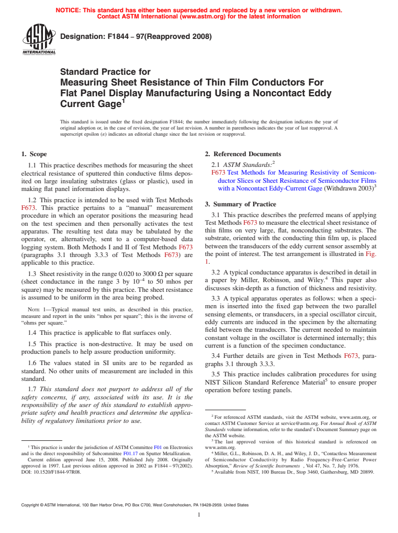
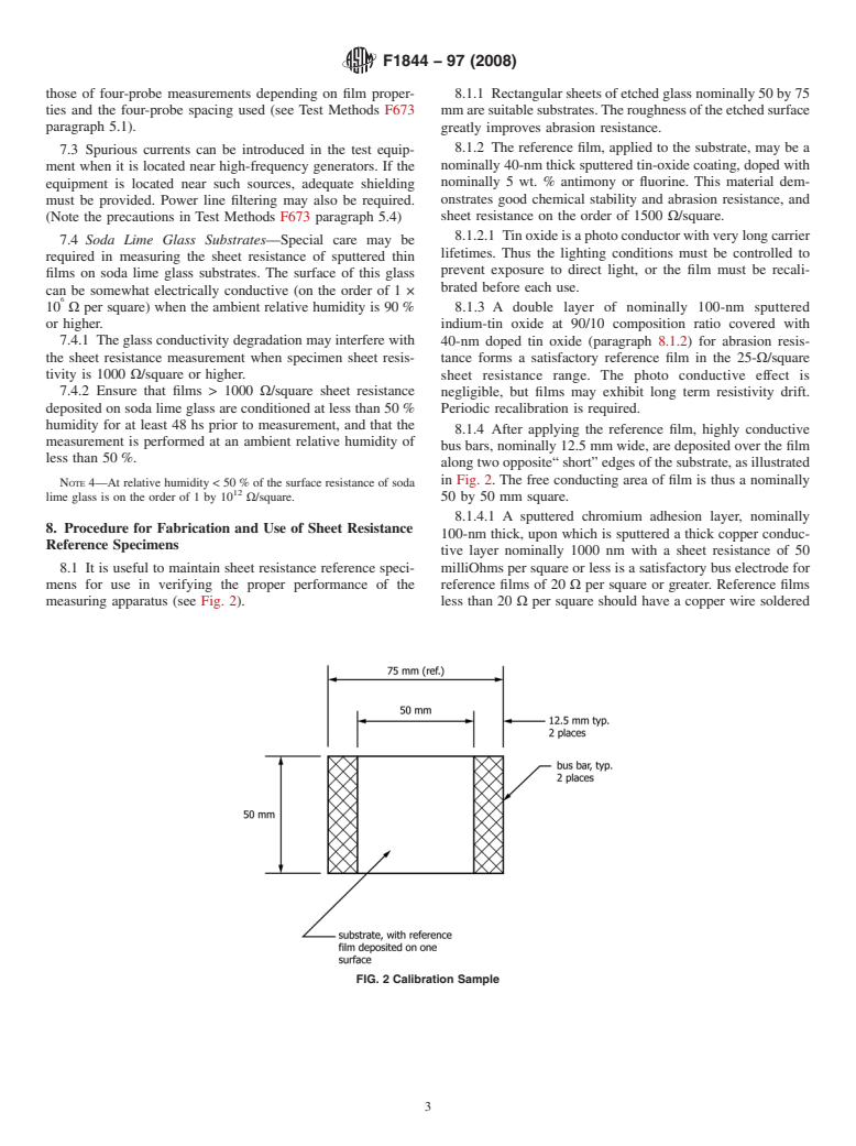
ASTM F1844-97(2008)
(Practice)Standard Practice for Measuring Sheet Resistance of Thin Film Conductors For Flat Panel Display Manufacturing Using a Noncontact Eddy Current Gage
Standard Practice for Measuring Sheet Resistance of Thin Film Conductors For Flat Panel Display Manufacturing Using a Noncontact Eddy Current Gage
SIGNIFICANCE AND USE
Resistivity is a primary quantity for characterization and specification of coated glass plates used for flat panel displays. Sheet resistance is also a primary quantity for characterization, specification, and monitoring of thin film fabrication processes.
This practice requires no specimen preparation.
The eddy current method is non-destructive to the thin film being measured. Special geometrical correction factors, needed for some four-point probe electrical resistivity measurements, are not required to derive the true sheet resistance so long as the transducers have a continuous layer of conductive thin film between them.
Test Methods F 673 refers to a testing arrangement in which the transducers and specimen (a semiconductor grade silicon wafer) are rigidly positioned. Similar apparatus is commercially available for testing large glass or plastic substrates, not envisioned in the scope of Test Methods F 673. A hand held probe can also be used, depending on throat depth required.
For use as a referee method, the probe and measuring apparatus must first be checked and qualified before use by the procedures of Test Methods F 673 (9.1.1 through 9.1.3 and 9.1.4.2 through 9.1.4.5), then this practice is used.
For use as a routine quality assurance method, this practice may be employed with periodic qualifications of probe and measuring apparatus by the procedures of Test Methods F 673 (9.1.1 through 9.1.3 and 9.1.4.2 through 9.1.4.5). The parties to the test must agree upon adequate qualification intervals for the test apparatus.
SCOPE
1.1 This practice describes methods for measuring the sheet electrical resistance of sputtered thin conductive films deposited on large insulating substrates (glass or plastic), used in making flat panel information displays.
1.2 This practice is intended to be used with Test Methods F 673. This practice pertains to a “manual” measurement procedure in which an operator positions the measuring head on the test specimen and then personally activates the test apparatus. The resulting test data may be tabulated by the operator, or, alternatively, sent to a computer-based data logging system. Both Methods I and II of Test Methods F 673 (paragraphs 3.1 through 3.3.3 of Test Methods F 673) are applicable to this practice.
1.3 Sheet resistivity in the range 0.020 to 3000 Ω per square (sheet conductance in the range 3 by 10–4 to 50 mhos per square) may be measured by this practice. The sheet resistance is assumed to be uniform in the area being probed.
Note 1—Typical manual test units, as described in this practice, measure and report in the units “mhos per square”; this is the inverse of “ohms per square.”
1.4 This practice is applicable to flat surfaces only.
1.5 This practice is non-destructive. It may be used on production panels to help assure production uniformity.
1.6 The values stated in SI units are to be regarded as standard. No other units of measurement are included in this standard.
1.7 This standard does not purport to address all of the safety concerns, if any, associated with its use. It is the responsibility of the user of this standard to establish appropriate safety and health practices and determine the applicability of regulatory limitations prior to use.
General Information
Relations
Standards Content (Sample)
NOTICE: This standard has either been superseded and replaced by a new version or withdrawn.
Contact ASTM International (www.astm.org) for the latest information
Designation: F1844 − 97(Reapproved 2008)
Standard Practice for
Measuring Sheet Resistance of Thin Film Conductors For
Flat Panel Display Manufacturing Using a Noncontact Eddy
Current Gage
This standard is issued under the fixed designation F1844; the number immediately following the designation indicates the year of
original adoption or, in the case of revision, the year of last revision.Anumber in parentheses indicates the year of last reapproval.A
superscript epsilon (´) indicates an editorial change since the last revision or reapproval.
1. Scope 2. Referenced Documents
2.1 ASTM Standards:
1.1 This practice describes methods for measuring the sheet
F673Test Methods for Measuring Resistivity of Semicon-
electrical resistance of sputtered thin conductive films depos-
ductor Slices or Sheet Resistance of Semiconductor Films
ited on large insulating substrates (glass or plastic), used in
withaNoncontactEddy-CurrentGage(Withdrawn2003)
making flat panel information displays.
1.2 This practice is intended to be used with Test Methods
3. Summary of Practice
F673. This practice pertains to a “manual” measurement
3.1 This practice describes the preferred means of applying
procedure in which an operator positions the measuring head
TestMethodsF673tomeasuretheelectricalsheetresistanceof
on the test specimen and then personally activates the test
thin films on very large, flat, nonconducting substrates. The
apparatus. The resulting test data may be tabulated by the
substrate, oriented with the conducting thin film up, is placed
operator, or, alternatively, sent to a computer-based data
betweenthetransducersoftheeddycurrentsensorassemblyat
logging system. Both Methods I and II of Test Methods F673
the point of interest. The test arrangement is illustrated in Fig.
(paragraphs 3.1 through 3.3.3 of Test Methods F673) are
1.
applicable to this practice.
3.2 Atypicalconductanceapparatusisdescribedindetailin
1.3 Sheetresistivityintherange0.020to3000Ωpersquare
–4
a paper by Miller, Robinson, and Wiley. This paper also
(sheet conductance in the range 3 by 10 to 50 mhos per
discusses skin-depth as a function of thickness and resistivity.
square) may be measured by this practice.The sheet resistance
is assumed to be uniform in the area being probed.
3.3 A typical apparatus operates as follows: when a speci-
men is inserted into the fixed gap between the two parallel
NOTE 1—Typical manual test units, as described in this practice,
sensing elements, or transducers, in a special oscillator circuit,
measure and report in the units “mhos per square”; this is the inverse of
“ohms per square.” eddy currents are induced in the specimen by the alternating
field between the transducers. The current needed to maintain
1.4 This practice is applicable to flat surfaces only.
constant voltage in the oscillator is determined internally; this
1.5 This practice is non-destructive. It may be used on
current is a function of the specimen conductance.
production panels to help assure production uniformity.
3.4 Further details are given in Test Methods F673, para-
1.6 The values stated in SI units are to be regarded as
graphs 3.1 through 3.3.3.
standard. No other units of measurement are included in this
3.5 This practice includes calibration procedures for using
standard.
NIST Silicon Standard Reference Material to ensure proper
1.7 This standard does not purport to address all of the
operation before testing panels.
safety concerns, if any, associated with its use. It is the
responsibility of the user of this standard to establish appro-
priate safety and health practices and determine the applica-
For referenced ASTM standards, visit the ASTM website, www.astm.org, or
bility of regulatory limitations prior to use.
contact ASTM Customer Service at service@astm.org. For Annual Book of ASTM
Standards volume information, refer to the standard’s Document Summary page on
the ASTM website.
The last approved version of this historical standard is referenced on
This practice is under the jurisdiction ofASTM Committee F01 on Electronics www.astm.org.
and is the direct responsibility of Subcommittee F01.17 on Sputter Metallization. Miller, G.L., Robinson, D.A. H., and Wiley, J. D., “Contactless Measurement
Current edition approved June 15, 2008. Published July 2008. Originally of Semiconductor Conductivity by Radio Frequency-Free-Carrier Power
approved in 1997. Last previous edition approved in 2002 as F1844–97(2002). Absorption,” Review of Scientific Instruments , Vol 47, No. 7, July 1976.
DOI: 10.1520/F1844-97R08. Available from NIST, 100 Bureau Dr., Stop 3460, Gaithersburg, MD 20899.
Copyright © ASTM International, 100 Barr Harbor Drive, PO Box C700, West Conshohocken, PA 19428-2959. United States
F1844 − 97 (2008)
5.1.1 Different transducer designs may be required to cover
the full range of sheet resistance values.
NOTE 2—Three transducers will generally cover the ranges of interest.
For convenience these are denoted “High” (15 to 3000 Ω per square),
“Low” (0.2 to 15 Ω per square) and “Extra Low” (0.035 to 0.2 Ω per
square).
NOTE 3—The usual “High” range transducer diameter is approximately
12.7 to 15.2 mm.The “Low” and “Extra Low” diameter is approximately
10.1to12.7mm.Averylargetransducer,63.5-mmdiameter,maybeused
forallrangesforthickerthannormalsubstrates(uptoapproximately2.54
mm) and for calibration and measurement ease.
5.2 Electrical Measuring Apparatus —The electrical appa-
ratus must meet the requirements of Test Methods F673,
paragraphs 6.1 through 6.4.
5.3 Specimen Support— The flat panel to be tested must be
supported firmly to ensure that the thin film is parallel with the
transducer surfaces.
5.4 Reagents and Materials in accordance with Test Meth-
ods F673, Section 7.
NOTE 1—This figure is partially copied from Fig. 1 of Test Methods
F673.
FIG. 1 Schematic Diagram of Eddy-Current Sensor Assembly 6. Test Specimen
6.1 The test article shall be a display substrate that has been
sputter coated with the conductive thin film of interest or ion
4. Significance and Use
implanted and annealed, or made conductive by another
process.
4.1 Resistivityisaprimaryquantityforcharacterizationand
specification of coated glass plates used for flat panel displays.
6.2 The conductive film must be thick enough that it is
Sheetresistanceisalsoaprimaryquantityforcharacterization,
continuous. Generally this requires that the film be at least
specification,andmonitoringofthinfilmfabricationprocesses.
15-nm thick.
4.2 This practice requires no specimen preparation.
6.3 The area to be tested shall be free of contamination and
mechanical damage, but shall not be cleaned or otherwise
4.3 The eddy current method is non-destructive to the thin
prepared.
film being measured. Special geometrical correction factors,
needed for some four-point probe electrical resistivity
6.4 Note that a sputtered film may also coat the edge of the
measurements, are not required to derive the true sheet
glass and can coat the back side of the substrate (“overspray”).
resistancesolongasthetransducershaveacontinuouslayerof
All overspray, for example, coating on back of glass, must be
conductive thin film between them.
removed before measurement.
4.4 Test Methods F673 refers to a testing arrangement in 6.4.1 Any remaining overspray will be included in the
which the transducers and specimen (a semiconductor grade measurement, lowering the measured film resistivity.
silicon wafer) are rigidly positioned. Similar apparatus is 6.4.2 Scribing the substrate near the edge using a glass
commercially available for testing large glass or plastic
scribe is not a reliable remedy.
substrates, not envisioned in the scope of Test Methods F673.
6.4.3 Useasimple2-pointprobeohmmetertoverifythatthe
Ahandheldprobecanalsobeused,dependingonthroatdepth
back side of glass or plastic substrate is insulating.
required.
7. Interferences
4.5 For use as a referee method, the probe and measuring
apparatusmustfirstbecheckedandqualifiedbeforeusebythe
7.1 Cautionmustbetakenthatthetransducergapisfixed,in
procedures of Test Methods F673 (9.1.1 through 9.1.3 and
accordance with the recommendations of the equipment sup-
9.1.4.2 through 9.1.4.5), then this practice is used.
plier. This may be ensured by firmly tightening the gap
adjustment screws after checking the spacing with gages. Use
4.6 For use as a routine quality assurance method, this
caution, too, that the electrostatic covers (see Miller, et. al. )
practicemaybeemployedwithperiodicqualificationsofprobe
arenotdamagedbythepanelundertest.Theelectrostaticcover
and measuring apparatus by the procedures of Test Methods
should be located approximately 0.02 mm below the support
F673 (9.1.1 through 9.1.3 and 9.1.4.2 through 9.1.4.5). The
surface.
parties to the test must agree upon adequate qualification
intervals for the test apparatus.
7.2 Radial resistivity variations or other resistivity nonuni-
formity under the transducer are averaged by this practice in a
5. Apparatus
manner that may be different from that of other types of
5.1 Eddy Current Sensor Assembly —See Fig. 1 and Test resistivity or sheet resistance techniques, which are responsive
Methods F673. to a finite lateral area. Th
...


Questions, Comments and Discussion
Ask us and Technical Secretary will try to provide an answer. You can facilitate discussion about the standard in here.