IEC TS 62607-6-17:2023
(Main)Nanomanufacturing - Key control characteristics - Part 6-17: Graphene-based material - Order parameter: X-ray diffraction and transmission electron microscopy
Nanomanufacturing - Key control characteristics - Part 6-17: Graphene-based material - Order parameter: X-ray diffraction and transmission electron microscopy
IEC TS 62607-6-17:2023 establishes a standardized method to determine the key control characteristic order parameter for graphene-based material and layered carbon material by X-ray diffraction (XRD) and transmission electron microscopy.
The order parameter is analysed from two perspectives: z-axis and x-y-axis. In the z-axis the order parameter is derived from the full width at half maximum (FWHM) of peak (002) in the XRD spectrum. In the x-y-axis, it is derived from the FWHM of peak (100) corresponding to diffraction patterns obtained by SAED (selected area electron diffraction) technique, which is routinely performed on most transmission electron microscopes in the world.
The method is applicable for graphene-based material and layered carbon material including graphite, expanded graphite, amorphous carbon, vitreous carbon or glassy carbon, the structures of which are clarified by other characterization techniques.
The method is applicable for differentiating few-layer graphene or reduced graphene oxide from layered carbon material.
Typical application area is quality control in manufacturing to ensure batch-to-batch reproducibility.
NOTE Graphene oxide, one type of graphene-based material, is not within the scope of this document.
General Information
- Status
- Published
- Publication Date
- 02-May-2023
- Technical Committee
- TC 113 - Nanotechnology for electrotechnical products and systems
- Drafting Committee
- WG 8 - TC 113/WG 8
- Current Stage
- PPUB - Publication issued
- Start Date
- 03-May-2023
- Completion Date
- 06-Jun-2023
Overview - IEC TS 62607-6-17:2023 (Graphene order parameter by XRD & TEM)
IEC TS 62607-6-17:2023 defines a standardized method for measuring the order parameter of graphene-based material and layered carbon materials using X‑ray diffraction (XRD) and transmission electron microscopy (TEM). The order parameter quantifies structural ordering from two perspectives:
- z‑axis: derived from the full width at half maximum (FWHM) of the (002) peak in XRD spectra;
- x–y axis: derived from the FWHM of the (100) peak from selected area electron diffraction (SAED) patterns recorded on TEM.
The specification applies to graphene-based and layered carbon materials (for example, graphite, expanded graphite, amorphous/vitreous/glassy carbon) whose basic structure has been characterized by other techniques. Graphene oxide is outside the scope.
Key topics and technical requirements
- Measurement principle: Bragg diffraction in XRD for z‑axis ordering; SAED for x–y ordering.
- Peaks used: FWHM of XRD (002) and SAED (100) peaks as the primary metrics for the order parameter.
- Instrumentation: requirements and descriptions for XRD and TEM equipment, sample preparation methods, and ambient conditions during measurement.
- Calibration and uncertainty: guidance on calibration protocols, sources of measurement uncertainty and how to address them.
- Data analysis and reporting: standardized analysis procedures, calculation of order parameters, and recommended report formats (including informative annexes and a case study for data interpretation).
- Applicability: method can differentiate few‑layer graphene or reduced graphene oxide from other layered carbon materials.
Applications - who uses this standard
- Manufacturers and process engineers - for quality control and to ensure batch‑to‑batch reproducibility in nanomanufacturing of graphene and carbon materials.
- Quality control and metrology laboratories - to implement repeatable XRD/TEM protocols and report consistent order‑parameter metrics.
- Materials scientists and R&D teams - for material classification, screening of few‑layer graphene, and correlating structural order with properties (e.g., thermal behavior).
- Standards committees and procurement teams - to specify testable acceptance criteria for graphene‑based products.
Practical value and SEO keywords
This Technical Specification supports robust, repeatable characterization of graphene-based material, enabling reliable use of order parameter, XRD, TEM, SAED, and FWHM metrics in manufacturing and research. Relevant keywords: IEC TS 62607-6-17:2023, graphene order parameter, graphene characterization, XRD (002) peak, TEM SAED (100) peak, layered carbon materials, quality control, nanomanufacturing.
Related standards
- Other parts of the IEC TS 62607 (Nanomanufacturing – Key control characteristics) series provide complementary methods and context for nanomaterial characterization and quality control.
Buy Documents
IEC TS 62607-6-17:2023 - Nanomanufacturing - Key control characteristics - Part 6-17: Graphene-based material - Order parameter: X-ray diffraction and transmission electron microscopy Released:5/3/2023 Isbn:9782832269411
Frequently Asked Questions
IEC TS 62607-6-17:2023 is a technical specification published by the International Electrotechnical Commission (IEC). Its full title is "Nanomanufacturing - Key control characteristics - Part 6-17: Graphene-based material - Order parameter: X-ray diffraction and transmission electron microscopy". This standard covers: IEC TS 62607-6-17:2023 establishes a standardized method to determine the key control characteristic order parameter for graphene-based material and layered carbon material by X-ray diffraction (XRD) and transmission electron microscopy. The order parameter is analysed from two perspectives: z-axis and x-y-axis. In the z-axis the order parameter is derived from the full width at half maximum (FWHM) of peak (002) in the XRD spectrum. In the x-y-axis, it is derived from the FWHM of peak (100) corresponding to diffraction patterns obtained by SAED (selected area electron diffraction) technique, which is routinely performed on most transmission electron microscopes in the world. The method is applicable for graphene-based material and layered carbon material including graphite, expanded graphite, amorphous carbon, vitreous carbon or glassy carbon, the structures of which are clarified by other characterization techniques. The method is applicable for differentiating few-layer graphene or reduced graphene oxide from layered carbon material. Typical application area is quality control in manufacturing to ensure batch-to-batch reproducibility. NOTE Graphene oxide, one type of graphene-based material, is not within the scope of this document.
IEC TS 62607-6-17:2023 establishes a standardized method to determine the key control characteristic order parameter for graphene-based material and layered carbon material by X-ray diffraction (XRD) and transmission electron microscopy. The order parameter is analysed from two perspectives: z-axis and x-y-axis. In the z-axis the order parameter is derived from the full width at half maximum (FWHM) of peak (002) in the XRD spectrum. In the x-y-axis, it is derived from the FWHM of peak (100) corresponding to diffraction patterns obtained by SAED (selected area electron diffraction) technique, which is routinely performed on most transmission electron microscopes in the world. The method is applicable for graphene-based material and layered carbon material including graphite, expanded graphite, amorphous carbon, vitreous carbon or glassy carbon, the structures of which are clarified by other characterization techniques. The method is applicable for differentiating few-layer graphene or reduced graphene oxide from layered carbon material. Typical application area is quality control in manufacturing to ensure batch-to-batch reproducibility. NOTE Graphene oxide, one type of graphene-based material, is not within the scope of this document.
IEC TS 62607-6-17:2023 is classified under the following ICS (International Classification for Standards) categories: 07.120 - Nanotechnologies. The ICS classification helps identify the subject area and facilitates finding related standards.
IEC TS 62607-6-17:2023 is available in PDF format for immediate download after purchase. The document can be added to your cart and obtained through the secure checkout process. Digital delivery ensures instant access to the complete standard document.
Standards Content (Sample)
IEC TS 62607-6-17 ®
Edition 1.0 2023-05
TECHNICAL
SPECIFICATION
colour
inside
Nanomanufacturing – Key control characteristics –
Part 6-17: Graphene-based material – Order parameter: X-ray diffraction and
transmission electron microscopy
All rights reserved. Unless otherwise specified, no part of this publication may be reproduced or utilized in any form
or by any means, electronic or mechanical, including photocopying and microfilm, without permission in writing from
either IEC or IEC's member National Committee in the country of the requester. If you have any questions about IEC
copyright or have an enquiry about obtaining additional rights to this publication, please contact the address below or
your local IEC member National Committee for further information.
IEC Secretariat Tel.: +41 22 919 02 11
3, rue de Varembé info@iec.ch
CH-1211 Geneva 20 www.iec.ch
Switzerland
About the IEC
The International Electrotechnical Commission (IEC) is the leading global organization that prepares and publishes
International Standards for all electrical, electronic and related technologies.
About IEC publications
The technical content of IEC publications is kept under constant review by the IEC. Please make sure that you have the
latest edition, a corrigendum or an amendment might have been published.
IEC publications search - webstore.iec.ch/advsearchform IEC Products & Services Portal - products.iec.ch
The advanced search enables to find IEC publications by a Discover our powerful search engine and read freely all the
variety of criteria (reference number, text, technical publications previews. With a subscription you will always have
committee, …). It also gives information on projects, replaced access to up to date content tailored to your needs.
and withdrawn publications.
Electropedia - www.electropedia.org
IEC Just Published - webstore.iec.ch/justpublished
The world's leading online dictionary on electrotechnology,
Stay up to date on all new IEC publications. Just Published
containing more than 22 300 terminological entries in English
details all new publications released. Available online and once
and French, with equivalent terms in 19 additional languages.
a month by email.
Also known as the International Electrotechnical Vocabulary
(IEV) online.
IEC Customer Service Centre - webstore.iec.ch/csc
If you wish to give us your feedback on this publication or need
further assistance, please contact the Customer Service
Centre: sales@iec.ch.
IEC TS 62607-6-17 ®
Edition 1.0 2023-05
TECHNICAL
SPECIFICATION
colour
inside
Nanomanufacturing – Key control characteristics –
Part 6-17: Graphene-based material – Order parameter: X-ray diffraction and
transmission electron microscopy
INTERNATIONAL
ELECTROTECHNICAL
COMMISSION
ICS 07.120 ISBN 978-2-8322-6941-1
– 2 – IEC TS 62607-6-17:2023 IEC 2023
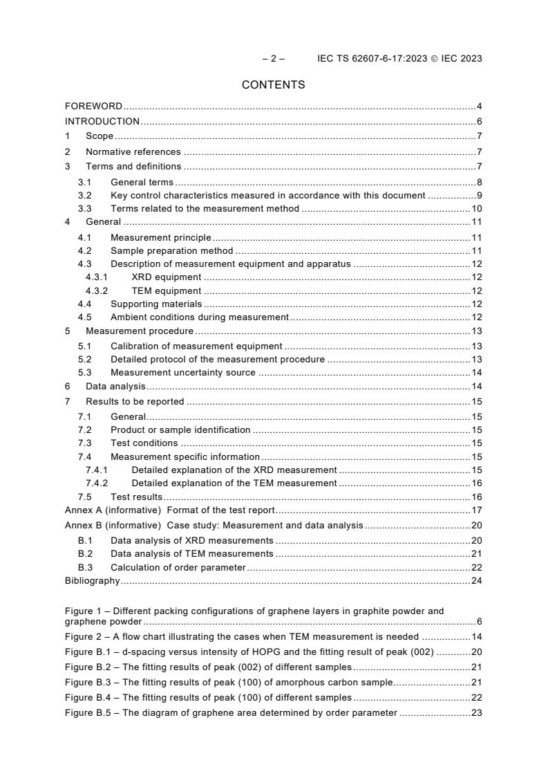
CONTENTS
FOREWORD . 4
INTRODUCTION . 6
1 Scope . 7
2 Normative references . 7
3 Terms and definitions . 7
3.1 General terms . 8
3.2 Key control characteristics measured in accordance with this document . 9
3.3 Terms related to the measurement method . 10
4 General . 11
4.1 Measurement principle . 11
4.2 Sample preparation method . 11
4.3 Description of measurement equipment and apparatus . 12
4.3.1 XRD equipment . 12
4.3.2 TEM equipment . 12
4.4 Supporting materials . 12
4.5 Ambient conditions during measurement . 12
5 Measurement procedure . 13
5.1 Calibration of measurement equipment . 13
5.2 Detailed protocol of the measurement procedure . 13
5.3 Measurement uncertainty source . 14
6 Data analysis . 14
7 Results to be reported . 15
7.1 General . 15
7.2 Product or sample identification . 15
7.3 Test conditions . 15
7.4 Measurement specific information . 15
7.4.1 Detailed explanation of the XRD measurement . 15
7.4.2 Detailed explanation of the TEM measurement . 16
7.5 Test results . 16
Annex A (informative) Format of the test report . 17
Annex B (informative) Case study: Measurement and data analysis . 20
B.1 Data analysis of XRD measurements . 20
B.2 Data analysis of TEM measurements . 21
B.3 Calculation of order parameter . 22
Bibliography . 24
Figure 1 – Different packing configurations of graphene layers in graphite powder and
graphene powder . 6
Figure 2 – A flow chart illustrating the cases when TEM measurement is needed . 14
Figure B.1 – d-spacing versus intensity of HOPG and the fitting result of peak (002) . 20
Figure B.2 – The fitting results of peak (002) of different samples . 21
Figure B.3 – The fitting results of peak (100) of amorphous carbon sample. 21
Figure B.4 – The fitting results of peak (100) of different samples . 22
Figure B.5 – The diagram of graphene area determined by order parameter . 23
Table A.1 – Product identification (in accordance with the relevant blank detail
specification) . 17
Table A.2 – General material description (in accordance with the relevant blank detail
specification) . 17
Table A.3 – Information related to XRD test . 18
Table A.4 – Information related to TEM test . 18
Table A.5 – Measurement results . 19
Table B.1 – Order parameters of different samples . 22
– 4 – IEC TS 62607-6-17:2023 IEC 2023
INTERNATIONAL ELECTROTECHNICAL COMMISSION
____________
NANOMANUFACTURING –
KEY CONTROL CHARACTERISTICS –
Part 6-17: Graphene-based material –
Order parameter: X-ray diffraction and transmission electron microscopy
FOREWORD
1) The International Electrotechnical Commission (IEC) is a worldwide organization for standardization comprising
all national electrotechnical committees (IEC National Committees). The object of IEC is to promote international
co-operation on all questions concerning standardization in the electrical and electronic fields. To this end and
in addition to other activities, IEC publishes International Standards, Technical Specifications, Technical Reports,
Publicly Available Specifications (PAS) and Guides (hereafter referred to as "IEC Publication(s)"). Their
preparation is entrusted to technical committees; any IEC National Committee interested in the subject dealt with
may participate in this preparatory work. International, governmental and non-governmental organizations liaising
with the IEC also participate in this preparation. IEC collaborates closely with the International Organization for
Standardization (ISO) in accordance with conditions determined by agreement between the two organizations.
2) The formal decisions or agreements of IEC on technical matters express, as nearly as possible, an international
consensus of opinion on the relevant subjects since each technical committee has representation from all
interested IEC National Committees.
3) IEC Publications have the form of recommendations for international use and are accepted by IEC National
Committees in that sense. While all reasonable efforts are made to ensure that the technical content of IEC
Publications is accurate, IEC cannot be held responsible for the way in which they are used or for any
misinterpretation by any end user.
4) In order to promote international uniformity, IEC National Committees undertake to apply IEC Publications
transparently to the maximum extent possible in their national and regional publications. Any divergence between
any IEC Publication and the corresponding national or regional publication shall be clearly indicated in the latter.
5) IEC itself does not provide any attestation of conformity. Independent certification bodies provide conformity
assessment services and, in some areas, access to IEC marks of conformity. IEC is not responsible for any
services carried out by independent certification bodies.
6) All users should ensure that they have the latest edition of this publication.
7) No liability shall attach to IEC or its directors, employees, servants or agents including individual experts and
members of its technical committees and IEC National Committees for any personal injury, property damage or
other damage of any nature whatsoever, whether direct or indirect, or for costs (including legal fees) and
expenses arising out of the publication, use of, or reliance upon, this IEC Publication or any other IEC
Publications.
8) Attention is drawn to the Normative references cited in this publication. Use of the referenced publications is
indispensable for the correct application of this publication.
9) Attention is drawn to the possibility that some of the elements of this IEC Publication may be the subject of patent
rights. IEC shall not be held responsible for identifying any or all such patent rights.
IEC TS 62607-6-17 has been prepared by IEC technical committee 113: Nanotechnology for
electrotechnical products and systems. It is a Technical Specification.
The text of this Technical Specification is based on the following documents:
Draft Report on voting
113/700/DTS 113/746/RVDTS
Full information on the voting for its approval can be found in the report on voting indicated in
the above table.
The language used for the development of this Technical Specification is English.
This document was drafted in accordance with ISO/IEC Directives, Part 2, and developed in
accordance with ISO/IEC Directives, Part 1 and ISO/IEC Directives, IEC Supplement, available
at www.iec.ch/members_experts/refdocs. The main document types developed by IEC are
described in greater detail at www.iec.ch/publications.
A list of all parts in the IEC TS 62607 series, published under the general title
Nanomanufacturing – Key control characteristics, can be found on the IEC website.
The committee has decided that the contents of this document will remain unchanged until the
stability date indicated on the IEC website under webstore.iec.ch in the data related to the
specific document. At this date, the document will be
• reconfirmed,
• withdrawn,
• replaced by a revised edition, or
• amended.
IMPORTANT – The "colour inside" logo on the cover page of this document indicates that it
contains colours which are considered to be useful for the correct understanding of its
contents. Users should therefore print this document using a colour printer.
– 6 – IEC TS 62607-6-17:2023 IEC 2023
INTRODUCTION
Graphite is composed of layers of carbon atoms just a single atom in thickness, known as
graphene layers, to which it owes many of its remarkable properties. When the thickness of
graphite flakes is reduced to just a few graphene layers, some of the material's technologically
most important characteristics are greatly enhanced. In other words, graphene is more than just
graphite. Although graphene has a vast number of potential applications, a survey of
commercially available graphene samples reveals that research could be undermined by the
poor quality of the available material [1] . Many highly priced graphene products from 60
producers consist mostly of graphite powder [2]. Therefore, a lack of classification standards is
creating a situation that downstream users are afraid to use graphene because they do not
know whether the graphene is fake.
Figure 1 shows the schematic packing configurations of graphene layers in graphite powder
(left side of Figure 1) and graphene powder (right side of Figure 1) and their corresponding
SEM images. It can be seen that graphite can be formed regularly in the z-axis, but graphene
powder is assembled like house-of-card-type stacking, which is formed by graphene layers in
a disorderly way in 3D space. For other carbon-related materials – for example, amorphous
carbon, glassy carbon, expanded graphite – their packing configurations differ from those of
graphite and graphene. An order parameter which indicates the order degree of a system can
be employed to classify different carbon-related materials.
Figure 1 – Different packing configurations of graphene layers
in graphite powder and graphene powder
This document establishes a method for determining the order parameter of graphene-based
material and carbon material. The order parameter can be analysed from the z-axis and x-y-axis,
respectively. The former can be derived from X-ray diffraction (XRD) spectra based on Bragg
diffraction, and the latter can be derived from the diffraction patterns by selected area electron
diffraction (SAED) technique, which is performed on a transmission electron microscope (TEM)
with very high-resolution imaging. Since thermal temperature can lead to re-graphitization, the
FWHM of peak (002) in the XRD spectrum indicates the quality of thermally reduced graphene
powder [3]. Therefore, the order parameter can be an index of production uniformity of
graphene-based materials, and also relates the materials' application with respect to heat
dissipation.
___________
Numbers in square brackets refer to the Bibliography.
NANOMANUFACTURING –
KEY CONTROL CHARACTERISTICS –
Part 6-17: Graphene-based material –
Order parameter: X-ray diffraction and transmission electron microscopy
1 Scope
This part of IEC TS 62607 establishes a standardized method to determine the key control
characteristic
– order parameter
for graphene-based material and layered carbon material by
– X-ray diffraction (XRD) and transmission electron microscopy.
The order parameter is analysed from two perspectives: z-axis and x-y-axis. In the z-axis the
order parameter is derived from the full width at half maximum (FWHM) of peak (002) in the
XRD spectrum. In the x-y-axis, it is derived from the FWHM of peak (100) corresponding to
diffraction patterns obtained by SAED (selected area electron diffraction) technique, which is
routinely performed on most transmission electron microscopes in the world.
– The method is applicable for graphene-based material and layered carbon material including
graphite, expanded graphite, amorphous carbon, vitreous carbon or glassy carbon, the
structures of which are clarified by other characterization techniques.
– The method is applicable for differentiating few-layer graphene or reduced graphene oxide
from layered carbon material.
– Typical application area is quality control in manufacturing to ensure batch-to-batch
reproducibility.
NOTE Graphene oxide, one type of graphene-based material, is not within the scope of this document.
2 Normative references
There are no normative references in this document.
3 Terms and definitions
For the purposes of this document, the following terms and definitions apply.
ISO and IEC maintain terminological databases for use in standardization at the following
addresses:
• IEC Electropedia: available at http://www.electropedia.org/
• ISO Online browsing platform: available at http://www.iso.org/obp
– 8 – IEC TS 62607-6-17:2023 IEC 2023
3.1 General terms
3.1.1
graphene
graphene layer
single layer graphene
monolayer graphene
single layer of carbon atoms with each atom bound to three neighbours in a honeycomb
structure
Note 1 to entry: It is an important building block of many carbon nano-objects.
Note 2 to entry: As graphene is a single layer, it is also sometimes called monolayer graphene or single-layer
graphene and abbreviated as 1LG to distinguish it from bilayer graphene (2LG) and few-layer graphene (FLG).
Note 3 to entry: Graphene has edges and can have defects and grain boundaries where the bonding is disrupted.
[SOURCE: ISO/TS 80004-13:2017, 3.1.2.1]
3.1.2
graphene-based material
GBM
graphene material grouping of carbon-based 2D materials that include one or more of graphene,
bilayer graphene, few-layer graphene, graphene nanoplate, and functionalized variations
thereof as well as graphene oxide and reduced graphene oxide
Note 1 to entry: "Graphene material" is a short name for graphene-based material.
3.1.3
few-layer graphene
FLG
two-dimensional material consisting of three to ten well-defined stacked graphene layers
[SOURCE: ISO/TS 80004-13:2017, 3.1.2.10]
3.1.4
reduced graphene oxide
rGO
reduced oxygen content form of graphene oxide
Note 1 to entry: This can be produced by chemical, thermal, microwave, photo-chemical, photo-thermal or
microbial/bacterial methods or by exfoliating reduced graphite oxide.
Note 2 to entry: If graphene oxide was fully reduced, then graphene would be the product. However, in practice,
3 2
some oxygen containing functional groups will remain and not all sp bonds will return back to sp configuration.
Different reducing agents will lead to different carbon to oxygen ratios and different chemical compositions in reduced
graphene oxide.
Note 3 to entry: It can take the form of several morphological variations such as platelets and worm-like structures.
[SOURCE: ISO/TS 80004-13:2017, 3.1.2.14]
3.1.5
graphite
allotropic form of the element carbon, consisting of graphene layers stacked parallel to each
other in a three-dimensional, crystalline, long-range order
Note 1 to entry: Adapted from the definition in the IUPAC Compendium of Chemical Terminology.
Note 2 to entry: There are two primary allotropic forms with different stacking arrangements: hexagonal and
rhombohedral.
[SOURCE: ISO/TS 80004-13:2017, 3.1.2.2]
3.1.6
highly oriented pyrolytic graphite
HOPG
highly pure and ordered form of synthetic graphite
Note 1 to entry: HOPG is often used as reference material for calibration of measurement equipment.
3.1.7
amorphous carbon
carbon material without long-range crystalline order
Note 1 to entry: Adapted from the definition in the IUPAC Compendium of Chemical Terminology.
Note 2 to entry: Short-range order exists, but with deviations of the interatomic distances or interbonding angles
with respect to the graphite lattice as well as to the diamond.
3.1.8
expanded graphite
modified graphite that has a layered structure with interlayer spacing
3.1.9
vitreous carbon
form of carbon derived through solid-phase carbonization from a preform comprising an
appropriate highly cross-linked polymer
Note 1 to entry: Vitreous carbon is characterized by a pseudo-amorphous, isotropic structure with low density, and
non-permeability for gases.
[SOURCE: ISO 20507:2022, 3.2.79]
3.1.10
key control characteristic
KCC
key performance indicator
material property or intermediate product characteristic which can affect safety or compliance
with regulations, fit, function, performance, quality, reliability or subsequent processing of the
final product
Note 1 to entry: The measurement of a key control characteristic is described in a standardized measurement
procedure with known accuracy and precision.
Note 2 to entry: It is possible to define more than one measurement method for a key control ch
...


Questions, Comments and Discussion
Ask us and Technical Secretary will try to provide an answer. You can facilitate discussion about the standard in here.
Loading comments...