ASTM F1892-12
(Guide)Standard Guide for Ionizing Radiation (Total Dose) Effects Testing of Semiconductor Devices
Standard Guide for Ionizing Radiation (Total Dose) Effects Testing of Semiconductor Devices
SIGNIFICANCE AND USE
5.1 Electronic circuits used in space, military, and nuclear power systems may be exposed to various levels of ionizing radiation. It is essential for the design and fabrication of such circuits that test methods be available that can determine the vulnerability or hardness (measure of nonvulnerability) of components to be used in such systems.
5.2 Some manufacturers currently are selling semiconductor parts with guaranteed hardness ratings. Use of this guide provides a basis for standardized qualification and acceptance testing.
SCOPE
1.1 This guide presents background and guidelines for establishing an appropriate sequence of tests and data analysis procedures for determining the ionizing radiation (total dose) hardness of microelectronic devices for dose rates below 300 rd(SiO2)/s. These tests and analysis will be appropriate to assist in the determination of the ability of the devices under test to meet specific hardness requirements or to evaluate the parts for use in a range of radiation environments.
1.2 The methods and guidelines presented will be applicable to characterization, qualification, and lot acceptance of silicon-based MOS and bipolar discrete devices and integrated circuits. They will be appropriate for treatment of the effects of electron and photon irradiation.
1.3 This guide provides a framework for choosing a test sequence based on general characteristics of the parts to be tested and the radiation hardness requirements or goals for these parts.
1.4 This guide provides for tradeoffs between minimizing the conservative nature of the testing method and minimizing the required testing effort.
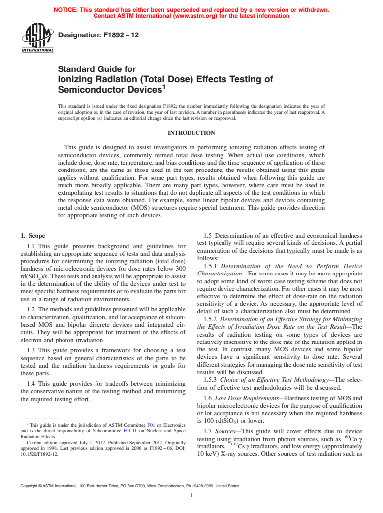
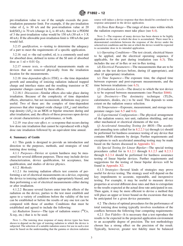
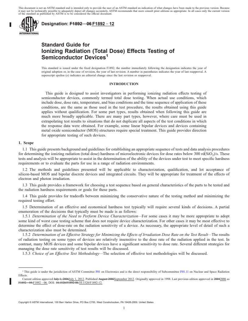
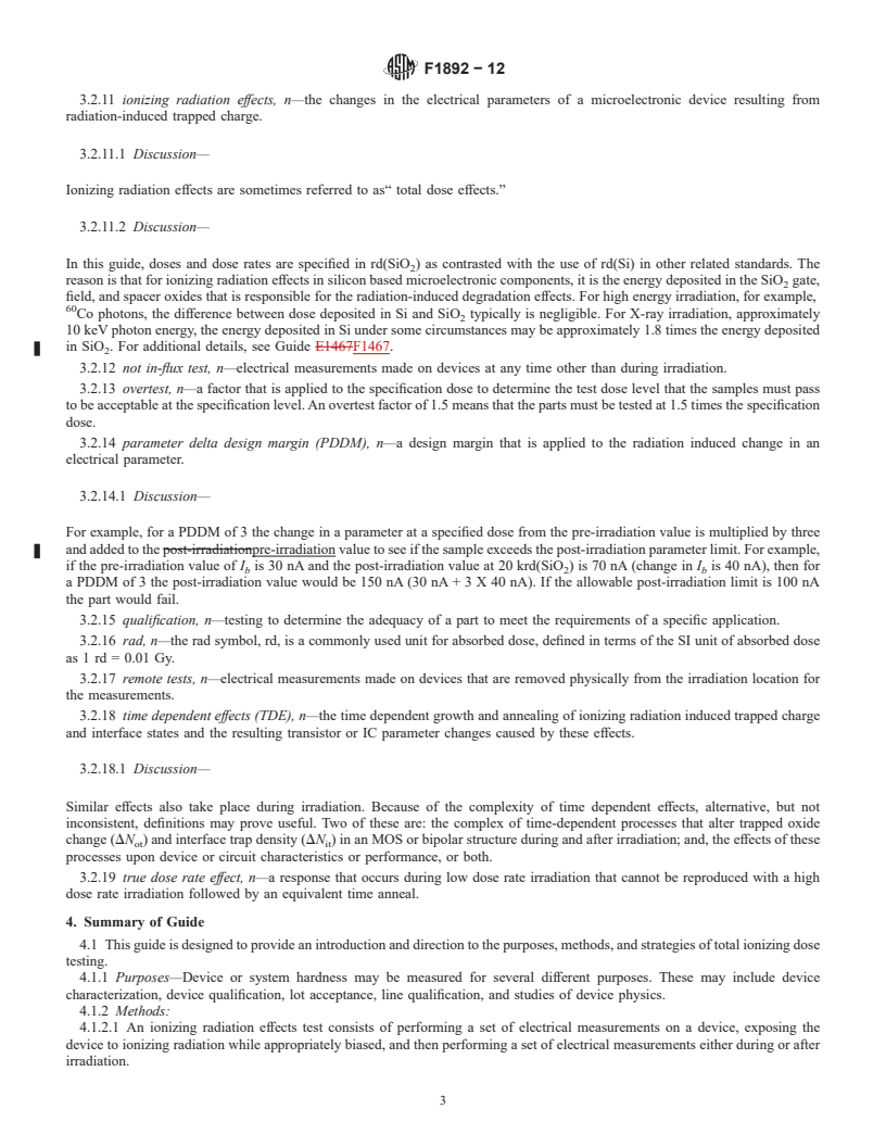
1.5 Determination of an effective and economical hardness test typically will require several kinds of decisions. A partial enumeration of the decisions that typically must be made is as follows:
1.5.1 Determination of the Need to Perform Device Characterization—For some cases it may be more appropriate to adopt some kind of worst case testing scheme that does not require device characterization. For other cases it may be most effective to determine the effect of dose-rate on the radiation sensitivity of a device. As necessary, the appropriate level of detail of such a characterization also must be determined.
1.5.2 Determination of an Effective Strategy for Minimizing the Effects of Irradiation Dose Rate on the Test Result—The results of radiation testing on some types of devices are relatively insensitive to the dose rate of the radiation applied in the test. In contrast, many MOS devices and some bipolar devices have a significant sensitivity to dose rate. Several different strategies for managing the dose rate sensitivity of test results will be discussed.
1.5.3 Choice of an Effective Test Methodology—The selection of effective test methodologies will be discussed.
1.6 Low Dose Requirements—Hardness testing of MOS and bipolar microelectronic devices for the purpose of qualification or lot acceptance is not necessary when the required hardness is 100 rd(SiO2) or lower.
1.7 Sources—This guide will cover effects due to device testing using irradiation from photon sources, such as 60Co γ irradiators, 137Cs γ irradiators, and low energy (approximately 10 keV) X-ray sources. Other sources of test radiation such as linacs, Van de Graaff sources, Dymnamitrons, SEMs, and flash X-ray sources occasionally are used but are outside the scope of this guide.
1.8 Displacement damage effects are outside the scope of this guide, as well.
1.9 The values stated in SI units are to be regarded as the standard.
General Information
Relations
Buy Standard
Standards Content (Sample)
NOTICE: This standard has either been superseded and replaced by a new version or withdrawn.
Contact ASTM International (www.astm.org) for the latest information
Designation: F1892 − 12
Standard Guide for
Ionizing Radiation (Total Dose) Effects Testing of
1
Semiconductor Devices
This standard is issued under the fixed designation F1892; the number immediately following the designation indicates the year of
original adoption or, in the case of revision, the year of last revision.Anumber in parentheses indicates the year of last reapproval.A
superscript epsilon (´) indicates an editorial change since the last revision or reapproval.
INTRODUCTION
This guide is designed to assist investigators in performing ionizing radiation effects testing of
semiconductor devices, commonly termed total dose testing. When actual use conditions, which
includedose,doserate,temperature,andbiasconditionsandthetimesequenceofapplicationofthese
conditions, are the same as those used in the test procedure, the results obtained using this guide
applies without qualification. For some part types, results obtained when following this guide are
much more broadly applicable. There are many part types, however, where care must be used in
extrapolating test results to situations that do not duplicate all aspects of the test conditions in which
the response data were obtained. For example, some linear bipolar devices and devices containing
metal oxide semiconductor (MOS) structures require special treatment. This guide provides direction
for appropriate testing of such devices.
1. Scope 1.5 Determination of an effective and economical hardness
test typically will require several kinds of decisions. A partial
1.1 This guide presents background and guidelines for
enumeration of the decisions that typically must be made is as
establishing an appropriate sequence of tests and data analysis
follows:
procedures for determining the ionizing radiation (total dose)
1.5.1 Determination of the Need to Perform Device
hardness of microelectronic devices for dose rates below 300
Characterization—For some cases it may be more appropriate
rd(SiO )/s.Thesetestsandanalysiswillbeappropriatetoassist
2
to adopt some kind of worst case testing scheme that does not
in the determination of the ability of the devices under test to
require device characterization. For other cases it may be most
meetspecifichardnessrequirementsortoevaluatethepartsfor
effective to determine the effect of dose-rate on the radiation
use in a range of radiation environments.
sensitivity of a device. As necessary, the appropriate level of
1.2 Themethodsandguidelinespresentedwillbeapplicable
detail of such a characterization also must be determined.
to characterization, qualification, and lot acceptance of silicon-
1.5.2 Determination of an Effective Strategy for Minimizing
based MOS and bipolar discrete devices and integrated cir-
the Effects of Irradiation Dose Rate on the Test Result—The
cuits. They will be appropriate for treatment of the effects of
results of radiation testing on some types of devices are
electron and photon irradiation.
relativelyinsensitivetothedoserateoftheradiationappliedin
the test. In contrast, many MOS devices and some bipolar
1.3 This guide provides a framework for choosing a test
devices have a significant sensitivity to dose rate. Several
sequence based on general characteristics of the parts to be
differentstrategiesformanagingthedoseratesensitivityoftest
tested and the radiation hardness requirements or goals for
results will be discussed.
these parts.
1.5.3 Choice of an Effective Test Methodology—The selec-
1.4 This guide provides for tradeoffs between minimizing
tion of effective test methodologies will be discussed.
the conservative nature of the testing method and minimizing
1.6 Low Dose Requirements—HardnesstestingofMOSand
the required testing effort.
bipolarmicroelectronicdevicesforthepurposeofqualification
or lot acceptance is not necessary when the required hardness
is 100 rd(SiO ) or lower.
2
1
This guide is under the jurisdiction of ASTM Committee F01 on Electronics
and is the direct responsibility of Subcommittee F01.11 on Nuclear and Space
1.7 Sources—This guide will cover effects due to device
Radiation Effects. 60
testing using irradiation from photon sources, such as Co γ
Current edition approved July 1, 2012. Published September 2012. Originally
137
irradiators, Csγirradiators,andlowenergy(approximately
approved in 1998. Last previous edition approved in 2006 as F1892–06. DOI:
10.1520/F1892-12. 10 keV) X-ray sources. Other sources of test radiation such as
Copyright © ASTM International, 100 Barr Harbor Drive, PO Box C700, West Conshohocken, PA 19428-2959. United States
1
---------------------- Page: 1 ----------------------
F1892 − 12
linacs,VandeGraaffsources,Dymnamitrons,SEMs,andflash 3.2.3 category B, n—used to refer to a part containing
X-ray sources occasionally are used but are outside the scope bipolar structures that is low dose rate
...
This document is not an ASTM standard and is intended only to provide the user of an ASTM standard an indication of what changes have been made to the previous version. Because
it may not be technically possible to adequately depict all changes accurately, ASTM recommends that users consult prior editions as appropriate. In all cases only the current version
of the standard as published by ASTM is to be considered the official document.
Designation: F1892 − 06 F1892 − 12
Standard Guide for
Ionizing Radiation (Total Dose) Effects Testing of
1
Semiconductor Devices
This standard is issued under the fixed designation F1892; the number immediately following the designation indicates the year of
original adoption or, in the case of revision, the year of last revision. A number in parentheses indicates the year of last reapproval. A
superscript epsilon (´) indicates an editorial change since the last revision or reapproval.
INTRODUCTION
This guide is designed to assist investigators in performing ionizing radiation effects testing of
semiconductor devices, commonly termed total dose testing. When actual use conditions, which
include dose, dose rate, temperature, and bias conditions and the time sequence of application of these
conditions, are the same as those used in the test procedure, the results obtained using this guide
applies without qualification. For some part types, results obtained when following this guide are
much more broadly applicable. There are many part types, however, where care must be used in
extrapolating test results to situations that do not duplicate all aspects of the test conditions in which
the response data were obtained. For example, some linear bipolar devices and devices containing
metal oxide semiconductor (MOS) structures require special treatment. This guide provides direction
for appropriate testing of such devices.
1. Scope
1.1 This guide presents background and guidelines for establishing an appropriate sequence of tests and data analysis procedures
for determining the ionizing radiation (total dose) hardness of microelectronic devices for dose rates below 300 rd(SiO )/s. These
2
tests and analysis will be appropriate to assist in the determination of the ability of the devices under test to meet specific hardness
requirements or to evaluate the parts for use in a range of radiation environments.
1.2 The methods and guidelines presented will be applicable to characterization, qualification, and lot acceptance of
silicon-based MOS and bipolar discrete devices and integrated circuits. They will be appropriate for treatment of the effects of
electron and photon irradiation.
1.3 This guide provides a framework for choosing a test sequence based on general characteristics of the parts to be tested and
the radiation hardness requirements or goals for these parts.
1.4 This guide provides for tradeoffs between minimizing the conservative nature of the testing method and minimizing the
required testing effort.
1.5 Determination of an effective and economical hardness test typically will require several kinds of decisions. A partial
enumeration of the decisions that typically must be made is as follows:
1.5.1 Determination of the Need to Perform Device Characterization—For some cases it may be more appropriate to adopt
some kind of worst case testing scheme that does not require device characterization. For other cases it may be most effective to
determine the effect of dose-rate on the radiation sensitivity of a device. As necessary, the appropriate level of detail of such a
characterization also must be determined.
1.5.2 Determination of an Effective Strategy for Minimizing the Effects of Irradiation Dose Rate on the Test Result—The results
of radiation testing on some types of devices are relatively insensitive to the dose rate of the radiation applied in the test. In
contrast, many MOS devices and some bipolar devices have a significant sensitivity to dose rate. Several different strategies for
managing the dose rate sensitivity of test results will be discussed.
1.5.3 Choice of an Effective Test Methodology—The selection of effective test methodologies will be discussed.
1
This guide is under the jurisdiction of ASTM Committee F01 on Electronics and is the direct responsibility of Subcommittee F01.11 on Nuclear and Space Radiation
Effects.
Current edition approved July 1, 2006July 1, 2012. Published August 2006September 2012. Originally approved in 1998. Last previous edition approved in 20042006 as
F1892 – 04.F1892 – 06. DOI: 10.1520/F1892-06.10.1520/F1892-12.
Copyright © ASTM International, 100 Barr Harbor Drive, PO Box C700, West Conshohocken, PA 19428-2959. United States
1
---------------------- Page: 1 ----------------------
F1892 − 12
1.6 Low Dose Requirements—Hardness testing of MOS and bipolar microelectronic devices for the purpose of qualification or
lot acceptance is not necessary when the required hardness is 100 rd(SiO ) or lower.
2
60
1.7 Sources—This guide will cover
...


Questions, Comments and Discussion
Ask us and Technical Secretary will try to provide an answer. You can facilitate discussion about the standard in here.