ASTM F1260-89
(Test Method)Test Method for Estimating Electromigration Median Time-To-Failure and Sigma of Integrated Circuit Metallizations
Test Method for Estimating Electromigration Median Time-To-Failure and Sigma of Integrated Circuit Metallizations
SCOPE
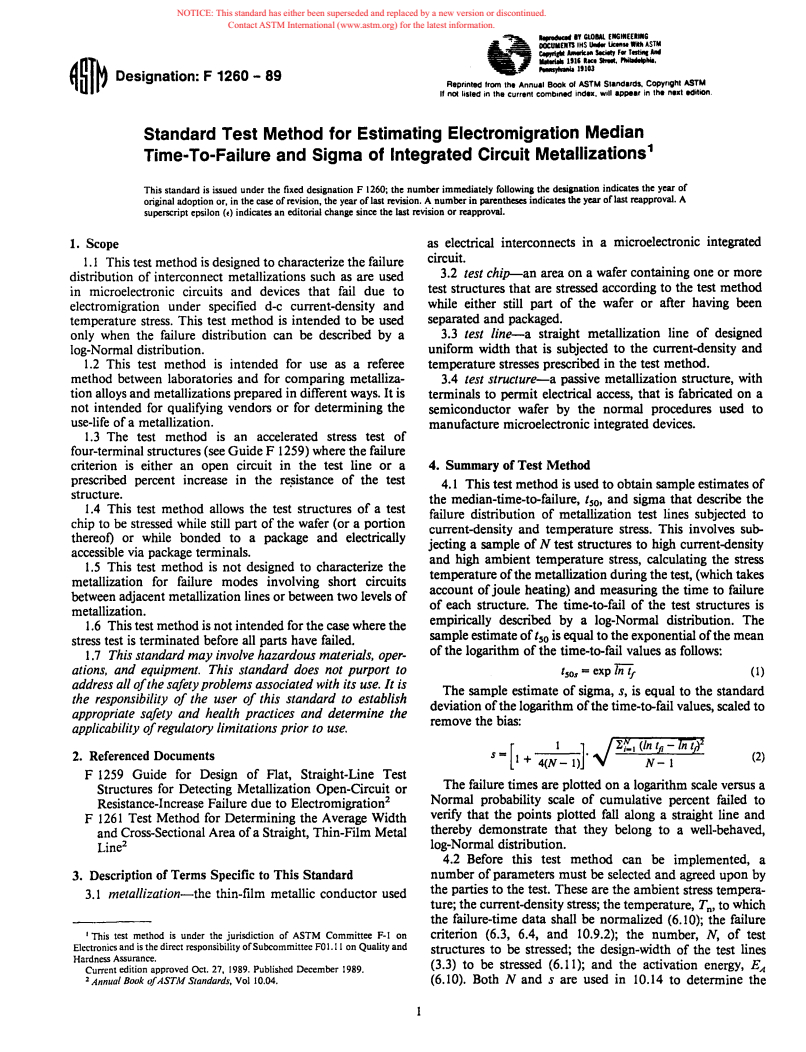
1.1 This test method is designed to characterize the failure distribution of interconnect metallizations such as are used in microelectronic circuits and devices that fail due to electromigration under specified d-c current-density and temperature stress. This test method is intended to be used only when the failure distribution can be described by a log-Normal distribution.
1.2 This test method is intended for use as a referee method between laboratories and for comparing metallization alloys and metallizations prepared in different ways. It is not intended for qualifying vendors or for determining the use-life of a metallization.
1.3 The test method is an accelerated stress test of four-terminal structures (see Guide F1259) where the failure criterion is either an open circuit in the test line or a prescribed percent increase in the resistance of the test structure.
1.4 This test method allows the test structures of a test chip to be stressed while still part of the wafer (or a portion thereof) or while bonded to a package and electrically accessible via package terminals.
1.5 This test method is not designed to characterize the metallization for failure modes involving short circuits between adjacent metallization lines or between two levels of metallization.
1.6 This test method is not intended for the case where the stress test is terminated before all parts have failed.
1.7 This standard may involve hazardous materials, operations, and equipment. This standard does not purport to address all of the safety problems associated with its use. It is the responsibility of the user of this standard to establish appropriate safety and health practices and determine the applicability of regulatory limitations prior to use.
General Information
Relations
Standards Content (Sample)
........ IT GlOllAl £11Gl1£EllllG
DOCU11£11l IHS lw. Uceost Wiiii ASTM
~-~ . S.Cilly F• latifll AN
....- ltl' ·--· Pllilldllpllio,
_,.1110J
~~l~ Designation: F 1260 - 89
Reprinted from the Annual Book of ASTM Standards, Copynght ASTM
If not listed in the current combined index, woll eppear in the next editiOn.
Standard Test Method for Estimating Electromigration Median
1
Time-To-Failure and Sigma of Integrated Circuit Metallizations
This standard is issued under the fixed designation F 1260; the number immediately following the designation indicates the year of
original adoption or, in the case of revision, the year of last revision. A number in parentheses indicates the year of last rcapproval. A
superscript epsilon (<) indicates an editorial change since the last revision or rcapproval.
as electrical interconnects in a microelectronic integrated
1. Scope
circuit.
I. I This test method is designed to characterize the failure
3.2 test chip-an area on a wafer containing one or more
distribution of interconnect metallizations such as are used
test structures that are stressed according to the test method
in microelectronic circuits and devices that fail due to
while either still part of the wafer or after having been
electromigration under specified d-c current-density and
separated and packaged.
temperature stress. This test method is intended to be used
3.3 test line-a straight metallization line of designed
only when the failure distribution can be described by a
uniform width that is subjected to the current-density and
log-Normal distribution.
I .2 This test method is intended for use as a referee temperature stresses prescribed in the test method.
method between laboratories and for comparing metalliza 3.4 test structure-a passive metallization structure, with
tion alloys and metallizations prepared in different ways. It is
terminals to permit electrical access, that is fabricated on a
not intended for qualifying vendors or for determining the
semiconductor wafer by the normal procedures used to
use-life of a metallization.
manufacture microelectronic integrated devices.
I .3 The test method is an accelerated stress test of
four-terminal structures (see Guide F I259) where the failure
4. Summary of Test Method
criterion is either an open circuit in the test line or a
prescribed percent increase in the re~istance of the test
4.1 This test method is used to obtain sample estimates of
structure.
the median-time-to-failure, t , and sigma that describe the
50
I .4 This test method allows the test structures of a test
failure distribution of metallization test lines subjected to
chip to be stressed while still part of the wafer (or a portion
current-density and temperature stress. This involves sub
thereoO or while bonded to a package and electrically
jecting a sample of N test structures to high current-density
accessible via package terminals.
and high ambient temperature stress, calculating the stress
1.5 This test method is not designed to characterize the
temperature of the metallization during the test, (which takes
metallization for failure modes involving short circuits
account of joule heating) and measuring the time to failure
between adjacent metallization lines or between two levels of
of each structure. The time-to-fail of the test structures is
metallization.
empirically described by a log-Normal distribution. The
1.6 This test method is not intended for the case where the
sample estimate of t is equal to the exponential of the mean
50
stress test is terminated before all parts have failed.
of the logarithm of the time-to-fail values as follows:
I .7 This standard may involve hazardous materials, oper
ations, and equipment. This standard does not purport to
t, s =exp In tf (1)
0
address all of the safety problems associated with its use. It is
The sample estimate of sigma, s, is equal to the standard
the responsibility of the user of this standard to establish
deviation of the logarithm of the time-to-fail values, scaled to
appropriate safety and health practices and determine the
remove the bias:
applicability of regulatory limitations prior to use.
s = [ I ]· / 2:f.t (In lg - tiip2
2. Referenced Documents (2)
I+ 4(N-1) '\f N-1
F I259 Guide for Design of Flat, Straight-Line Test
The failure times are plotted on a logarithm scale versus a
Structures for Detecting Metallization Open-Circuit or
2
Normal probability scale of cumulative percent failed to
Resistance-Increase Failure due to Electromigration
verify that the points plotted fall along a straight line and
F I26I Test Method for Determining the Average Width
thereby demonstrate that they belong to a well-behaved,
and Cross-Sectional Area of a Straight, Thin-Film Metal
2
log-Normal distribution.
Line
4.2 Before this test method can be implemented, a
3. Description of Terms Specific to This Standard number of parameters must be selected and agre
...


Questions, Comments and Discussion
Ask us and Technical Secretary will try to provide an answer. You can facilitate discussion about the standard in here.