EN 62417:2010
(Main)Semiconductor devices - Mobile ion tests for metal-oxide semiconductor field effect transistors (MOSFETs)
Semiconductor devices - Mobile ion tests for metal-oxide semiconductor field effect transistors (MOSFETs)
IEC 62417:2010 provides a wafer level test procedure to determine the amount of positive mobile charge in oxide layers in metal-oxide semiconductor field effect transistors. It is applicable to both active and parasitic field effect transistors. The mobile charge can cause degradation of microelectronic devices, e.g. by shifting the threshold voltage of MOSFETs or by inversion of the base in bipolar transistors.
Halbleiterbauelemente - Prüfverfahren auf mobile Ionen für Feldeffekttransistoren mit Metall-Oxid-Halbleiter (MOSFET)
Dispositifs à semiconducteurs - Essais d'ions mobiles pour transistors à semiconducteur à oxyde métallique à effet de champ (MOSFET)
La CEI 62417:2010 fournit une procédure d'essai au niveau de la plaquette pour déterminer la quantité de charge positive mobile à l'intérieur des couches d'oxyde dans les transistors à semiconducteur à oxyde métallique à effet de champ. Elle s'applique aux deux transistors à effets parasites et effets actifs. La charge mobile peut causer des dégradations des dispositifs microélectroniques, par exemple en décalant la tension de seuil des MOSFETs ou par inversion de la base dans les transistors bipolaires.
Polprevodniški elementi - Preskusi z mobilnimi ioni tranzistorjev s kovinskim oksidom na poljski efekt (MOSFET) (IEC 62417:2010)
Pričujoči standard zagotavlja postopek preskušanja na ploščici za ugotavljanje količine pozitivnega mobilnega naboja v oksidnih plasteh tranzistorjev s kovinskim oksidom na poljski efekt. Velja za aktivne in parazitne tranzistorje na poljski efekt. Mobilni naboj lahko povzroči razpad mikroelektronskih naprav, npr. s premikom mejne napetosti tranzistorjev s kovinskim oksidom na poljski efekt ali z inverzijo osnovnih in bipolarnih tranzistorjev.
General Information
- Status
- Published
- Publication Date
- 06-May-2010
- Withdrawal Date
- 30-Apr-2013
- Technical Committee
- CLC/TC 47X - Semiconductor devices and trusted chips
- Drafting Committee
- IEC/TC 47 - IEC_TC_47
- Parallel Committee
- IEC/TC 47 - IEC_TC_47
- Current Stage
- 6060 - Document made available - Publishing
- Start Date
- 07-May-2010
- Completion Date
- 07-May-2010
Overview
EN 62417:2010, titled "Semiconductor devices - Mobile ion tests for metal-oxide semiconductor field effect transistors (MOSFETs)," is a European standard developed by CLC and based on the international IEC 62417:2010. This standard specifies a wafer-level test procedure for detecting and quantifying positive mobile ions within oxide layers of MOSFET devices. The presence of mobile ions can cause detrimental effects such as threshold voltage shifts in MOSFETs or inversion of the base in bipolar transistors, leading to device degradation. This standard applies to both active and parasitic field effect transistors, ensuring reliability and quality assurance in semiconductor device manufacturing.
Key Topics
- Mobile ion detection in MOSFET oxides
Establishes procedures to measure positive mobile charge that affects device performance and longevity. - Test methods
- Bias Temperature Stress (BTS): Involves applying a gate bias at elevated temperature (up to 250 °C) to mobilize ions and measuring threshold voltage shifts via I-V or capacitance-voltage (C-V) measurements before and after stress.
- Voltage Sweep (VS): Uses quasi-static and low frequency C-V measurements on capacitors to identify ionic displacement currents, indicating mobile ion concentration.
- Test equipment
Requires hot chuck capable of up to 250 °C, LCR meter for high-frequency C-V, pA-meter for low-frequency measurements, and precision voltage supplies. - Test conditions and sample size
Specifies electric field strengths depending on gate materials (up to ±1 MV/cm) and recommends a minimum sample size of five. - Criteria for acceptance
Defines maximum allowable threshold voltage shifts (e.g., less than 0.02 × maximum supply voltage or specific limits based on gate type), ensuring device stability against mobile ion effects. - Reporting requirements
Enforces comprehensive documentation of test setups, sample sizes, measured shifts, and any deviations from prescribed conditions.
Applications
EN 62417:2010 is vital for semiconductor manufacturers and quality control laboratories involved in production and testing of MOSFET devices. By standardizing mobile ion testing:
- It ensures device reliability by detecting contamination or defects in oxide layers that can cause threshold voltage drift.
- It supports process control during semiconductor fabrication by providing clear criteria and methods to monitor oxide quality.
- It aids in failure analysis and product qualification, helping design robust MOSFETs for applications in consumer electronics, automotive, industrial, and communication sectors.
- The standard also benefits suppliers of semiconductor materials, enabling verification of oxide integrity prior to device integration.
Related Standards
- IEC 60747 Series - Semiconductor devices standards covering device terminology and generic measurement techniques, complementing EN 62417.
- IEC 60384-1 - Fixed capacitors for electronic equipment relevant for capacitor structures used in the voltage sweep test.
- ISO/IEC Directives, Part 2 - Framework for developing international standards, including IEC 62417.
- Industry-specific electrical test standards which may incorporate mobile ion testing as part of device qualification protocols.
Keywords: MOSFET mobile ion test, EN 62417:2010, IEC 62417, threshold voltage shift, bias temperature stress, voltage sweep, semiconductor device testing, oxide layer contamination, electrical characterization, device reliability.
Frequently Asked Questions
EN 62417:2010 is a standard published by CLC. Its full title is "Semiconductor devices - Mobile ion tests for metal-oxide semiconductor field effect transistors (MOSFETs)". This standard covers: IEC 62417:2010 provides a wafer level test procedure to determine the amount of positive mobile charge in oxide layers in metal-oxide semiconductor field effect transistors. It is applicable to both active and parasitic field effect transistors. The mobile charge can cause degradation of microelectronic devices, e.g. by shifting the threshold voltage of MOSFETs or by inversion of the base in bipolar transistors.
IEC 62417:2010 provides a wafer level test procedure to determine the amount of positive mobile charge in oxide layers in metal-oxide semiconductor field effect transistors. It is applicable to both active and parasitic field effect transistors. The mobile charge can cause degradation of microelectronic devices, e.g. by shifting the threshold voltage of MOSFETs or by inversion of the base in bipolar transistors.
EN 62417:2010 is classified under the following ICS (International Classification for Standards) categories: 31.080 - Semiconductor devices. The ICS classification helps identify the subject area and facilitates finding related standards.
EN 62417:2010 is available in PDF format for immediate download after purchase. The document can be added to your cart and obtained through the secure checkout process. Digital delivery ensures instant access to the complete standard document.
Standards Content (Sample)
SLOVENSKI STANDARD
01-september-2010
Polprevodniški elementi - Preskusi z mobilnimi ioni tranzistorjev s kovinskim
oksidom na poljski efekt (MOSFET) (IEC 62417:2010)
Semiconductor devices - Mobile ion tests for metal-oxide semiconductor field effect
transistors (MOSFETs) (IEC 62417:2010)
Halbleiterbauelemente - Prüfverfahren auf mobile Ionen für Feldeffekttransistoren mit
Metall-Oxid-Halbleiter (MOSFET) (IEC 62417:2010)
Dispositifs à semiconducteurs - Essais d'ions mobiles pour transistors à semiconducteur
à oxyde métallique à effet de champ (MOSFET) (CEI 62417:2010)
Ta slovenski standard je istoveten z: EN 62417:2010
ICS:
31.080.01 Polprevodniški elementi Semiconductor devices in
(naprave) na splošno general
2003-01.Slovenski inštitut za standardizacijo. Razmnoževanje celote ali delov tega standarda ni dovoljeno.
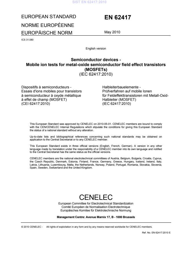
EUROPEAN STANDARD
EN 62417
NORME EUROPÉENNE
May 2010
EUROPÄISCHE NORM
ICS 31.080
English version
Semiconductor devices -
Mobile ion tests for metal-oxide semiconductor field effect transistors
(MOSFETs)
(IEC 62417:2010)
Dispositifs à semiconducteurs - Halbleiterbauelemente -
Essais d'ions mobiles pour transistors Prüfverfahren auf mobile Ionen
à semiconducteur à oxyde métallique für Feldeffekttransistoren mit Metall-Oxid-
à effet de champ (MOSFET) Halbleiter (MOSFET)
(CEI 62417:2010) (IEC 62417:2010)
This European Standard was approved by CENELEC on 2010-05-01. CENELEC members are bound to comply
with the CEN/CENELEC Internal Regulations which stipulate the conditions for giving this European Standard
the status of a national standard without any alteration.
Up-to-date lists and bibliographical references concerning such national standards may be obtained on
application to the Central Secretariat or to any CENELEC member.
This European Standard exists in three official versions (English, French, German). A version in any other
language made by translation under the responsibility of a CENELEC member into its own language and notified
to the Central Secretariat has the same status as the official versions.
CENELEC members are the national electrotechnical committees of Austria, Belgium, Bulgaria, Croatia, Cyprus,
the Czech Republic, Denmark, Estonia, Finland, France, Germany, Greece, Hungary, Iceland, Ireland, Italy,
Latvia, Lithuania, Luxembourg, Malta, the Netherlands, Norway, Poland, Portugal, Romania, Slovakia, Slovenia,
Spain, Sweden, Switzerland and the United Kingdom.
CENELEC
European Committee for Electrotechnical Standardization
Comité Européen de Normalisation Electrotechnique
Europäisches Komitee für Elektrotechnische Normung
Management Centre: Avenue Marnix 17, B - 1000 Brussels
© 2010 CENELEC - All rights of exploitation in any form and by any means reserved worldwide for CENELEC members.
Ref. No. EN 62417:2010 E
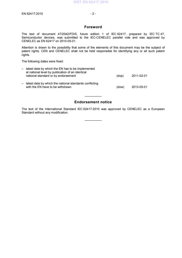
Foreword
The text of document 47/2042/FDIS, future edition 1 of IEC 62417, prepared by IEC TC 47,
Semiconductor devices, was submitted to the IEC-CENELEC parallel vote and was approved by
CENELEC as EN 62417 on 2010-05-01.
Attention is drawn to the possibility that some of the elements of this document may be the subject of
patent rights. CEN and CENELEC shall not be held responsible for identifying any or all such patent
rights.
The following dates were fixed:
– latest date by which the EN has to be implemented
at national level by publication of an identical
(dop) 2011-02-01
national standard or by endorsement
– latest date by which the national standards conflicting
(dow) 2013-05-01
with the EN have to be withdrawn
__________
Endorsement notice
The text of the International Standard IEC 62417:2010 was approved by CENELEC as a European
Standard without any modification.
__________
IEC 62417 ®
Edition 1.0 2010-04
INTERNATIONAL
STANDARD
NORME
INTERNATIONALE
Semiconductor devices – Mobile ion tests for metal-oxide semiconductor field
effect transistors (MOSFETs)
Dispositifs à semiconducteurs – Essais d’ions mobiles pour transistors à
semiconducteur à oxyde métallique à effet de champ (MOSFETs)
INTERNATIONAL
ELECTROTECHNICAL
COMMISSION
COMMISSION
ELECTROTECHNIQUE
PRICE CODE
INTERNATIONALE
H
CODE PRIX
ICS 31.080 ISBN 978-2-88910-696-7
– 2 – 62417 © IEC:2010
CONTENTS
FOREWORD.3
1 Scope.5
2 Abbreviations and letter symbols .5
3 General description .5
4 Test equipment.6
5 Test structures .6
6 Sample size.6
7 Conditions .6
8 Procedure .7
8.1 Bias temperature stress.7
8.2 Voltage sweep.7
9 Criteria .7
10 Reporting .8
62417 © IEC:2010 – 3 –
INTERNATIONAL ELECTROTECHNICAL COMMISSION
____________
SEMICONDUCTOR DEVICES –
MOBILE ION TESTS FOR METAL-OXIDE
SEMICONDUCTOR FIELD EFFECT
TRANSISTORS (MOSFETs)
FOREWORD
1) The International Electrotechnical Commission (IEC) is a worldwide organization for standardization comprising
all national electrotechnical committees (IEC National Committees). The object of IEC is to promote
international co-operation on all questions concerning standardization in the electrical and electronic fields. To
this end and in addition to other activities, IEC publishes International Standards, Technical Specifications,
Technical Reports, Publicly Available Specifications (PAS) and Guides (hereafter referred to as “IEC
Publication(s)”). Their preparation is entrusted to technical committees; any IEC National Committee interested
in the subject dealt with may participate in this preparatory work. International, governmental and non-
governmental organizations liaising with the IEC also participate in this preparation. IEC collaborates closely
with the International Organization for Standardization (ISO) in accordance with conditions determined by
agreement between the two organizations.
2) The formal decisions or agreements of IEC on technical matters express, as nearly as possible, an international
consensus of opinion on the relevant subjects since each technical committee has representation from all
interested IEC National Committees.
3) IEC Publications have the form of recommendations for international use and are accepted by IEC National
Committees in that sense. While all reasonable efforts are made to ensure that the technical content of IEC
Publications is accurate, IEC cannot be held responsible for the way in which they are used or for any
misinterpretation by any end user.
4) In order to promote international uniformity, IEC National Committees undertake to apply IEC Publications
transparently to the maximum extent possible in their national and regional publications. Any divergence
between any IEC Publication and the corresponding national or regional publication shall be clearly indicated in
the latter.
5) IEC itself does not provide any attestation of conformity. Independent certification bodies provide conformity
assessment services and, in some areas, access to IEC marks of conformity. IEC is not responsible for any
services carried out by independent certification bodies.
6) All users should ensure that they have the latest edition of this publication.
7) No liability shall attach to IEC or its directors, employees, servants or agents including individual experts and
members of its technical committees and IEC National Committees for any personal injury, property damage or
other damage of any nature whatsoever, whether direct or indirect, or for costs (including legal fees) and
expenses arising out of the publication, use of, or reliance upon, this IEC Publication or any other IEC
Publications.
8) Attention is drawn to the Normative references cited in this public
...


Questions, Comments and Discussion
Ask us and Technical Secretary will try to provide an answer. You can facilitate discussion about the standard in here.
Loading comments...