ASTM F1893-18
(Guide)Guide for Measurement of Ionizing Dose-Rate Survivability and Burnout of Semiconductor Devices (Withdrawn 2023)
Guide for Measurement of Ionizing Dose-Rate Survivability and Burnout of Semiconductor Devices (Withdrawn 2023)
SIGNIFICANCE AND USE
5.1 The use of FXR or LINAC radiation sources for the determination of high dose-rate burnout in semiconductor devices is addressed in this guide. The goal of this guide is to provide a systematic approach to testing semiconductor devices for burnout or survivability.
5.2 The different types of failure modes that are possible are defined and discussed in this guide. Specifically, failure can be defined by a change in device parameters, or by a catastrophic failure of the device.
5.3 This guide can be used to determine if a device survives (that is, continues to operate and function within the specified performance parameters) when irradiated to a predetermined dose-rate level; or, the guide can be used to determine the dose-rate burnout failure level (that is, the minimum dose rate at which burnout failure occurs). However, since this latter test is destructive, the minimum dose-rate burnout failure level must be determined statistically.
SCOPE
1.1 This guide defines the detailed requirements for testing semiconductor devices for short-pulse high dose-rate ionization-induced survivability and burnout failure. The test facility shall be capable of providing the necessary dose rates to perform the measurements. Typically, large flash X-ray (FXR) machines operated in the photon mode, or FXR e-beam facilities are utilized because of their high dose-rate capabilities. Electron Linear Accelerators (LINACs) may be used if the dose rate is sufficient. Two modes of test are described: (1) A survivability test, and (2) A burnout failure level test.
1.2 The values stated in International System of Units (SI) are to be regarded as standard. No other units of measurement are included in this standard.
1.3 This international standard was developed in accordance with internationally recognized principles on standardization established in the Decision on Principles for the Development of International Standards, Guides and Recommendations issued by the World Trade Organization Technical Barriers to Trade (TBT) Committee.
WITHDRAWN RATIONALE
This guide defines the detailed requirements for testing semiconductor devices for short-pulse high dose-rate ionization-induced survivability and burnout failure. The test facility shall be capable of providing the necessary dose rates to perform the measurements. Typically, large flash X-ray (FXR) machines operated in the photon mode, or FXR e-beam facilities are utilized because of their high dose-rate capabilities. Electron Linear Accelerators (LINACs) may be used if the dose rate is sufficient. Two modes of test are described: (1) A survivability test, and (2) A burnout failure level test.
Formerly under the jurisdiction of Committee F01 on Electronics, this guide was withdrawn in November 2023. This standard is being withdrawn without replacement because Committee F01 was disbanded.
General Information
Relations
Buy Standard
Standards Content (Sample)
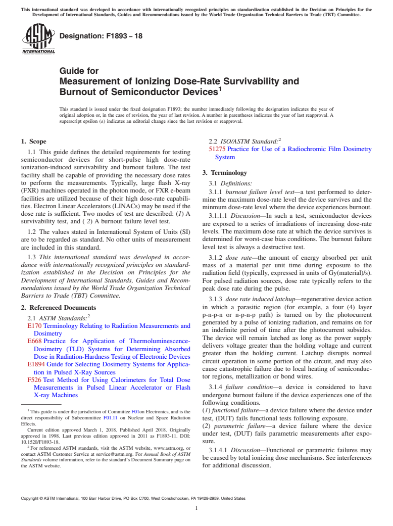
This international standard was developed in accordance with internationally recognized principles on standardization established in the Decision on Principles for the
Development of International Standards, Guides and Recommendations issued by the World Trade Organization Technical Barriers to Trade (TBT) Committee.
Designation: F1893 − 18
Guide for
Measurement of Ionizing Dose-Rate Survivability and
1
Burnout of Semiconductor Devices
This standard is issued under the fixed designation F1893; the number immediately following the designation indicates the year of
original adoption or, in the case of revision, the year of last revision.Anumber in parentheses indicates the year of last reapproval.A
superscript epsilon (´) indicates an editorial change since the last revision or reapproval.
2
1. Scope 2.2 ISO/ASTM Standard:
51275Practice for Use of a Radiochromic Film Dosimetry
1.1 This guide defines the detailed requirements for testing
System
semiconductor devices for short-pulse high dose-rate
ionization-induced survivability and burnout failure. The test
3. Terminology
facility shall be capable of providing the necessary dose rates
to perform the measurements. Typically, large flash X-ray
3.1 Definitions:
(FXR) machines operated in the photon mode, or FXR e-beam
3.1.1 burnout failure level test—a test performed to deter-
facilities are utilized because of their high dose-rate capabili-
mine the maximum dose-rate level the device survives and the
ties.ElectronLinearAccelerators(LINACs)maybeusedifthe
minmumdose-ratelevelwherethedeviceexperiencesburnout.
dose rate is sufficient. Two modes of test are described: (1)A
3.1.1.1 Discussion—In such a test, semiconductor devices
survivability test, and ( 2) A burnout failure level test.
are exposed to a series of irradiations of increasing dose-rate
levels.The maximum dose rate at which the device survives is
1.2 The values stated in International System of Units (SI)
determined for worst-case bias conditions. The burnout failure
are to be regarded as standard. No other units of measurement
level test is always a destructive test.
are included in this standard.
1.3 This international standard was developed in accor- 3.1.2 dose rate—the amount of energy absorbed per unit
dance with internationally recognized principles on standard-
mass of a material per unit time during exposure to the
ization established in the Decision on Principles for the radiation field (typically, expressed in units of Gy(material)/s).
Development of International Standards, Guides and Recom-
For pulsed radiation sources, dose rate typically refers to the
mendations issued by the World Trade Organization Technical peak dose rate during the pulse.
Barriers to Trade (TBT) Committee.
3.1.3 dose rate induced latchup—regenerativedeviceaction
in which a parasitic region (for example, a four (4) layer
2. Referenced Documents
p-n-p-n or n-p-n-p path) is turned on by the photocurrent
2
2.1 ASTM Standards:
generated by a pulse of ionizing radiation, and remains on for
E170Terminology Relating to Radiation Measurements and
an indefinite period of time after the photocurrent subsides.
Dosimetry
The device will remain latched as long as the power supply
E668 Practice for Application of Thermoluminescence-
delivers voltage greater than the holding voltage and current
Dosimetry (TLD) Systems for Determining Absorbed
greater than the holding current. Latchup disrupts normal
DoseinRadiation-HardnessTestingofElectronicDevices
circuit operation in some portion of the circuit, and may also
E1894Guide for Selecting Dosimetry Systems forApplica-
cause catastrophic failure due to local heating of semiconduc-
tion in Pulsed X-Ray Sources
tor regions, metallization or bond wires.
F526Test Method for Using Calorimeters for Total Dose
3.1.4 failure condition—a device is considered to have
Measurements in Pulsed Linear Accelerator or Flash
undergone burnout failure if the device experiences one of the
X-ray Machines
following conditions.
1
(1) functional failure—a device failure where the device under
ThisguideisunderthejurisdictionofCommitteeF01onElectronics,andisthe
direct responsibility of Subcommittee F01.11 on Nuclear and Space Radiation
test, (DUT) fails functional tests following exposure.
Effects.
(2) parametric failure—a device failure where the device
Current edition approved March 1, 2018. Published April 2018. Originally
under test, (DUT) fails parametric measurements after expo-
approved in 1998. Last previous edition approved in 2011 as F1893-11. DOI:
10.1520/F1893-18. sure.
2
For referenced ASTM standards, visit the ASTM website, www.astm.org, or
3.1.4.1 Discussion—Functional or parametric failures may
contact ASTM Customer Service at service@astm.org. For Annual Book of ASTM
becausedbytotalionizingdosemechanisms.Seeinterferences
Standards volume information, refer to the standard’s Document Summary page on
the ASTM website. for additional discussion.
Copyright © ASTM International, 100 Barr Harbor Drive, PO Bo
...
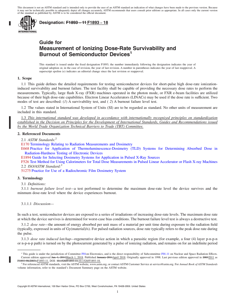
This document is not an ASTM standard and is intended only to provide the user of an ASTM standard an indication of what changes have been made to the previous version. Because
it may not be technically possible to adequately depict all changes accurately, ASTM recommends that users consult prior editions as appropriate. In all cases only the current version
of the standard as published by ASTM is to be considered the official document.
Designation: F1893 − 11 F1893 − 18
Guide for
Measurement of Ionizing Dose-Rate Survivability and
1
Burnout of Semiconductor Devices
This standard is issued under the fixed designation F1893; the number immediately following the designation indicates the year of
original adoption or, in the case of revision, the year of last revision. A number in parentheses indicates the year of last reapproval. A
superscript epsilon (´) indicates an editorial change since the last revision or reapproval.
1. Scope
1.1 This guide defines the detailed requirements for testing semiconductor devices for short-pulse high dose-rate ionization-
induced survivability and burnout failure. The test facility shall be capable of providing the necessary dose rates to perform the
measurements. Typically, large flash X-ray (FXR) machines operated in the photon mode, or FXR e-beam facilities are utilized
because of their high dose-rate capabilities. Electron Linear Accelerators (LINACs) may be used if the dose rate is sufficient. Two
modes of test are described: (1) A survivability test, and ( 2) A burnout failure level test.
1.2 The values stated in International System of Units (SI) are to be regarded as standard. No other units of measurement are
included in this standard.
1.3 This international standard was developed in accordance with internationally recognized principles on standardization
established in the Decision on Principles for the Development of International Standards, Guides and Recommendations issued
by the World Trade Organization Technical Barriers to Trade (TBT) Committee.
2. Referenced Documents
2
2.1 ASTM Standards:
E170 Terminology Relating to Radiation Measurements and Dosimetry
E668 Practice for Application of Thermoluminescence-Dosimetry (TLD) Systems for Determining Absorbed Dose in
Radiation-Hardness Testing of Electronic Devices
E1894 Guide for Selecting Dosimetry Systems for Application in Pulsed X-Ray Sources
F526 Test Method for Using Calorimeters for Total Dose Measurements in Pulsed Linear Accelerator or Flash X-ray Machines
2
2.2 ISO/ASTM Standard:
51275 Practice for Use of a Radiochromic Film Dosimetry System
3. Terminology
3.1 Definitions:
3.1.1 burnout failure level test—a test performed to determine the maximum dose-rate level the device survives and the
minmum dose-rate level where the device experiences burnout.
3.1.1.1 Discussion—
In such a test, semiconductor devices are exposed to a series of irradiations of increasing dose-rate levels. The maximum dose rate
at which the device survives is determined for worst-case bias conditions. The burnout failure level test is always a destructive test.
3.1.2 dose rate—the amount of energy absorbed per unit mass of a material per unit time during exposure to the radiation field
(typically, expressed in units of Gy(material)/s). For pulsed radiation sources, dose rate typically refers to the peak dose rate during
the pulse.
3.1.3 dose rate induced latchup—regenerative device action in which a parasitic region (for example, a four (4) layer p-n-p-n
or n-p-n-p path) is turned on by the photocurrent generated by a pulse of ionizing radiation, and remains on for an indefinite period
1
This guide is under the jurisdiction of Committee F01on Electronics, and is the direct responsibility of Subcommittee F01.11 on Nuclear and Space Radiation Effects.
Current edition approved Jan. 1, 2011March 1, 2018. Published January 2011April 2018. Originally approved in 1998. Last previous edition approved in 20032011 as
F1893-98(2003).F1893-11. DOI: 10.1520/F1893-11.10.1520/F1893-18.
2
For referenced ASTM standards, visit the ASTM website, www.astm.org, or contact ASTM Customer Service at service@astm.org. For Annual Book of ASTM Standards
volume information, refer to the standard’s Document Summary page on the ASTM website.
Copyright © ASTM International, 100 Barr Harbor Drive, PO Box C700, West Conshohocken, PA 19428-2959. United States
1
---------------------- Page: 1 ----------------------
F1893 − 18
of time after the photocurrent subsides. The device will remain latched as long as the power supply delivers voltage greater than
the holding voltage and current greater than the holding current. Latchup disrupts normal circuit operation in some portion of the
circuit, and may also cause catastrophic failure due to local heating of semiconductor regions, metallization or bond wires.
3.1.4 failure condition—a device is considered to have undergone burnout failure if the device experiences one of the following
conditions.
(1) functional failure—a de
...
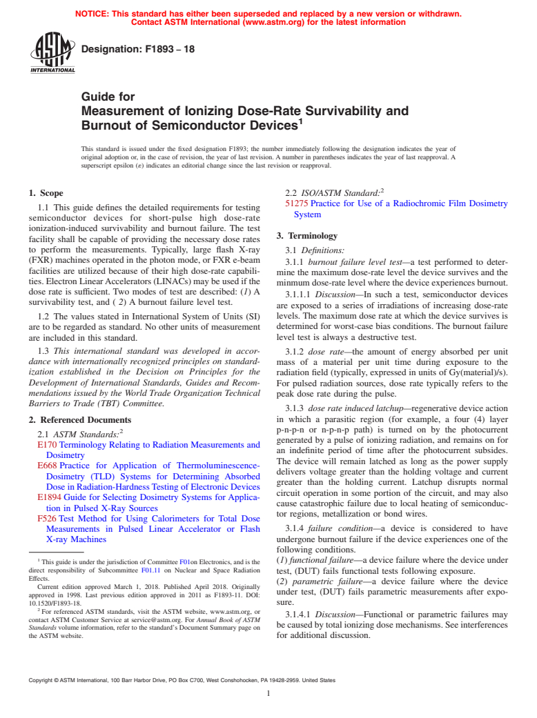
NOTICE: This standard has either been superseded and replaced by a new version or withdrawn.
Contact ASTM International (www.astm.org) for the latest information
Designation: F1893 − 18
Guide for
Measurement of Ionizing Dose-Rate Survivability and
1
Burnout of Semiconductor Devices
This standard is issued under the fixed designation F1893; the number immediately following the designation indicates the year of
original adoption or, in the case of revision, the year of last revision. A number in parentheses indicates the year of last reapproval. A
superscript epsilon (´) indicates an editorial change since the last revision or reapproval.
2
1. Scope 2.2 ISO/ASTM Standard:
51275 Practice for Use of a Radiochromic Film Dosimetry
1.1 This guide defines the detailed requirements for testing
System
semiconductor devices for short-pulse high dose-rate
ionization-induced survivability and burnout failure. The test
3. Terminology
facility shall be capable of providing the necessary dose rates
to perform the measurements. Typically, large flash X-ray 3.1 Definitions:
(FXR) machines operated in the photon mode, or FXR e-beam
3.1.1 burnout failure level test—a test performed to deter-
facilities are utilized because of their high dose-rate capabili-
mine the maximum dose-rate level the device survives and the
ties. Electron Linear Accelerators (LINACs) may be used if the
minmum dose-rate level where the device experiences burnout.
dose rate is sufficient. Two modes of test are described: (1) A
3.1.1.1 Discussion—In such a test, semiconductor devices
survivability test, and ( 2) A burnout failure level test.
are exposed to a series of irradiations of increasing dose-rate
levels. The maximum dose rate at which the device survives is
1.2 The values stated in International System of Units (SI)
determined for worst-case bias conditions. The burnout failure
are to be regarded as standard. No other units of measurement
level test is always a destructive test.
are included in this standard.
1.3 This international standard was developed in accor-
3.1.2 dose rate—the amount of energy absorbed per unit
dance with internationally recognized principles on standard- mass of a material per unit time during exposure to the
ization established in the Decision on Principles for the
radiation field (typically, expressed in units of Gy(material)/s).
Development of International Standards, Guides and Recom- For pulsed radiation sources, dose rate typically refers to the
mendations issued by the World Trade Organization Technical
peak dose rate during the pulse.
Barriers to Trade (TBT) Committee.
3.1.3 dose rate induced latchup—regenerative device action
in which a parasitic region (for example, a four (4) layer
2. Referenced Documents
2 p-n-p-n or n-p-n-p path) is turned on by the photocurrent
2.1 ASTM Standards:
generated by a pulse of ionizing radiation, and remains on for
E170 Terminology Relating to Radiation Measurements and
an indefinite period of time after the photocurrent subsides.
Dosimetry
The device will remain latched as long as the power supply
E668 Practice for Application of Thermoluminescence-
delivers voltage greater than the holding voltage and current
Dosimetry (TLD) Systems for Determining Absorbed
greater than the holding current. Latchup disrupts normal
Dose in Radiation-Hardness Testing of Electronic Devices
circuit operation in some portion of the circuit, and may also
E1894 Guide for Selecting Dosimetry Systems for Applica-
cause catastrophic failure due to local heating of semiconduc-
tion in Pulsed X-Ray Sources
tor regions, metallization or bond wires.
F526 Test Method for Using Calorimeters for Total Dose
3.1.4 failure condition—a device is considered to have
Measurements in Pulsed Linear Accelerator or Flash
X-ray Machines undergone burnout failure if the device experiences one of the
following conditions.
1
(1) functional failure—a device failure where the device under
This guide is under the jurisdiction of Committee F01on Electronics, and is the
direct responsibility of Subcommittee F01.11 on Nuclear and Space Radiation
test, (DUT) fails functional tests following exposure.
Effects.
(2) parametric failure—a device failure where the device
Current edition approved March 1, 2018. Published April 2018. Originally
under test, (DUT) fails parametric measurements after expo-
approved in 1998. Last previous edition approved in 2011 as F1893-11. DOI:
10.1520/F1893-18. sure.
2
For referenced ASTM standards, visit the ASTM website, www.astm.org, or
3.1.4.1 Discussion—Functional or parametric failures may
contact ASTM Customer Service at service@astm.org. For Annual Book of ASTM
be caused by total ionizing dose mechanisms. See interferences
Standards volume information, refer to the standard’s Document Summary page on
the ASTM website. for additional discussion.
Copyright © ASTM International, 100 Barr Harbor Drive, PO Box C700, West Conshohocken, PA 19428-2959. United States
1
---------------------- Page: 1 -----
...



Questions, Comments and Discussion
Ask us and Technical Secretary will try to provide an answer. You can facilitate discussion about the standard in here.