IEC 62899-503-1:2020
(Main)Printed electronics - Part 503-1: Quality assessment - Test method of displacement current measurement for printed thin-film transistor
Printed electronics - Part 503-1: Quality assessment - Test method of displacement current measurement for printed thin-film transistor
IEC 62899-503-1:2020(E) specifies a test method for displacement current measurement (DCM) for printed thin film transistors (TFTs) or organic thin film transistors (OTFTs).
General Information
- Status
- Published
- Publication Date
- 26-May-2020
- Technical Committee
- TC 119 - Printed Electronics
- Drafting Committee
- WG 5 - TC 119/WG 5
- Current Stage
- PPUB - Publication issued
- Start Date
- 27-May-2020
- Completion Date
- 19-Jun-2020
Overview
IEC 62899-503-1:2020 defines a standardized test method for displacement current measurement (DCM) applied to printed thin-film transistors (printed TFTs) and organic thin-film transistors (OTFTs). The standard describes the measurement setup, environmental conditioning, measurement procedure and reporting requirements used to characterize carrier behavior, charge trapping and channel capacitance in printed electronics. It is part of the IEC 62899 series on printed electronics and was prepared by IEC TC 119.
Key topics and requirements
- Scope: Specifies DCM for printed TFTs / OTFTs as a direct method to detect charge motion between source/channel/drain and gate.
- Measurement principle: Apply a triangular gate voltage waveform and record source and drain currents (I_S and I_D) versus gate-to-source voltage (U_GS). Compute displacement current (I_dis), trapped charge (Q_trap and ΔQ_trap) and injected/ejected carrier charges.
- Apparatus: Typical instruments include a function generator, amplifier, oscilloscope and low-noise power/battery, plus an electronic measurement kit to minimize external parasitic capacitance introduced by probes and cables.
- Procedure highlights:
- Mount specimen per figure and wiring schema in the standard.
- Apply triangle wave with constant amplitude and frequency to the gate.
- Measure I vs U for source and drain, calculate displacement current and integrate to obtain charges and channel capacitance.
- Use Annex A for charge trapping and channel capacitance measurement details.
- Environmental conditions: Conditioning and testing atmospheres per ISO 291 - generally (23 ± 2) °C and (50 ± 10) % RH; tighter class-1 conditions for plastic substrates (23 ± 1 °C, 50 ± 5 % RH).
- Reporting: Include experimental conditions, data formats, measured symbols (e.g., Q_trap, C_channel), and test frequency dependence.
Applications and users
IEC 62899-503-1 is intended for:
- R&D teams characterizing carrier injection, trapping and mobility in printed/organic semiconductors.
- Quality assurance and process control for printed TFT manufacturing.
- Materials and ink suppliers validating semiconductor or dielectric performance.
- Test labs and conformity assessors evaluating device reliability and electrical properties.
- Designers of flexible electronics, sensors, displays and other printed-electronics products who require quantitative channel-capacitance and trapping metrics.
Practical benefits include standardized, repeatable DCM measurements that help troubleshoot contact injection issues, evaluate dielectric/semiconductor interfaces, and compare device batches.
Related standards
- IEC 62899 series (Printed electronics) - other parts cover component and quality assessment topics (see IEC webstore for the full list).
- ISO 291 - referenced normative standard for conditioning and test atmospheres.
Keywords: IEC 62899-503-1, displacement current measurement, DCM, printed TFT, OTFT, charge trapping, channel capacitance, printed thin-film transistor, printed electronics.
Get Certified
Connect with accredited certification bodies for this standard

Intertek Testing Services NA Inc.
Intertek certification services in North America.

UL Solutions
Global safety science company with testing, inspection and certification.

ANCE
Mexican certification and testing association.
Sponsored listings
Frequently Asked Questions
IEC 62899-503-1:2020 is a standard published by the International Electrotechnical Commission (IEC). Its full title is "Printed electronics - Part 503-1: Quality assessment - Test method of displacement current measurement for printed thin-film transistor". This standard covers: IEC 62899-503-1:2020(E) specifies a test method for displacement current measurement (DCM) for printed thin film transistors (TFTs) or organic thin film transistors (OTFTs).
IEC 62899-503-1:2020(E) specifies a test method for displacement current measurement (DCM) for printed thin film transistors (TFTs) or organic thin film transistors (OTFTs).
IEC 62899-503-1:2020 is classified under the following ICS (International Classification for Standards) categories: 01.040.29 - Electrical engineering (Vocabularies); 29.045 - Semiconducting materials; 29.240 - Power transmission and distribution networks; 31.080.30 - Transistors. The ICS classification helps identify the subject area and facilitates finding related standards.
IEC 62899-503-1:2020 is available in PDF format for immediate download after purchase. The document can be added to your cart and obtained through the secure checkout process. Digital delivery ensures instant access to the complete standard document.
Standards Content (Sample)
IEC 62899-503-1 ®
Edition 1.0 2020-05
INTERNATIONAL
STANDARD
colour
inside
Printed electronics –
Part 503-1: Quality assessment – Test method of displacement current
measurement for printed thin-film transistor
All rights reserved. Unless otherwise specified, no part of this publication may be reproduced or utilized in any form
or by any means, electronic or mechanical, including photocopying and microfilm, without permission in writing from
either IEC or IEC's member National Committee in the country of the requester. If you have any questions about IEC
copyright or have an enquiry about obtaining additional rights to this publication, please contact the address below or
your local IEC member National Committee for further information.
IEC Central Office Tel.: +41 22 919 02 11
3, rue de Varembé info@iec.ch
CH-1211 Geneva 20 www.iec.ch
Switzerland
About the IEC
The International Electrotechnical Commission (IEC) is the leading global organization that prepares and publishes
International Standards for all electrical, electronic and related technologies.
About IEC publications
The technical content of IEC publications is kept under constant review by the IEC. Please make sure that you have the
latest edition, a corrigendum or an amendment might have been published.
IEC publications search - webstore.iec.ch/advsearchform Electropedia - www.electropedia.org
The advanced search enables to find IEC publications by a The world's leading online dictionary on electrotechnology,
variety of criteria (reference number, text, technical containing more than 22 000 terminological entries in English
committee,…). It also gives information on projects, replaced and French, with equivalent terms in 16 additional languages.
and withdrawn publications. Also known as the International Electrotechnical Vocabulary
(IEV) online.
IEC Just Published - webstore.iec.ch/justpublished
Stay up to date on all new IEC publications. Just Published IEC Glossary - std.iec.ch/glossary
details all new publications released. Available online and 67 000 electrotechnical terminology entries in English and
once a month by email. French extracted from the Terms and Definitions clause of
IEC publications issued since 2002. Some entries have been
IEC Customer Service Centre - webstore.iec.ch/csc collected from earlier publications of IEC TC 37, 77, 86 and
If you wish to give us your feedback on this publication or CISPR.
need further assistance, please contact the Customer Service
Centre: sales@iec.ch.
IEC 62899-503-1 ®
Edition 1.0 2020-05
INTERNATIONAL
STANDARD
colour
inside
Printed electronics –
Part 503-1: Quality assessment – Test method of displacement current
measurement for printed thin-film transistor
INTERNATIONAL
ELECTROTECHNICAL
COMMISSION
ICS 29.045; 31.080.30 ISBN 978-2-8322-8378-3
– 2 – IEC 62899-503-1:2020 © IEC 2020
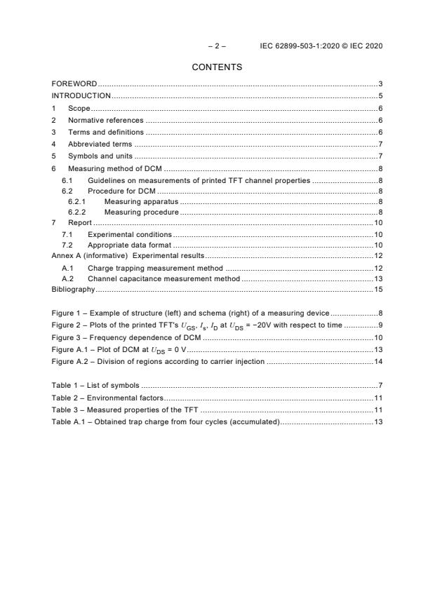
CONTENTS
FOREWORD . 3
INTRODUCTION . 5
1 Scope . 6
2 Normative references . 6
3 Terms and definitions . 6
4 Abbreviated terms . 7
5 Symbols and units . 7
6 Measuring method of DCM . 8
6.1 Guidelines on measurements of printed TFT channel properties . 8
6.2 Procedure for DCM . 8
6.2.1 Measuring apparatus . 8
6.2.2 Measuring procedure . 8
7 Report . 10
7.1 Experimental conditions . 10
7.2 Appropriate data format . 10
Annex A (informative) Experimental results . 12
A.1 Charge trapping measurement method . 12
A.2 Channel capacitance measurement method . 13
Bibliography . 15
Figure 1 – Example of structure (left) and schema (right) of a measuring device . 8
Figure 2 – Plots of the printed TFT's U , I , I at U = −20V with respect to time . 9
GS s D DS
Figure 3 – Frequency dependence of DCM . 10
Figure A.1 – Plot of DCM at U = 0 V . 13
DS
Figure A.2 – Division of regions according to carrier injection . 14
Table 1 – List of symbols . 7
Table 2 – Environmental factors . 11
Table 3 – Measured properties of the TFT . 11
Table A.1 – Obtained trap charge from four cycles (accumulated) . 13
INTERNATIONAL ELECTROTECHNICAL COMMISSION
____________
PRINTED ELECTRONICS –
Part 503-1: Quality assessment –
Test method of displacement current
measurement for printed thin-film transistor
FOREWORD
1) The International Electrotechnical Commission (IEC) is a worldwide organization for standardization comprising
all national electrotechnical committees (IEC National Committees). The object of IEC is to promote
international co-operation on all questions concerning standardization in the electrical and electronic fields. To
this end and in addition to other activities, IEC publishes International Standards, Technical Specifications,
Technical Reports, Publicly Available Specifications (PAS) and Guides (hereafter referred to as “IEC
Publication(s)”). Their preparation is entrusted to technical committees; any IEC National Committee interested
in the subject dealt with may participate in this preparatory work. International, governmental and non-
governmental organizations liaising with the IEC also participate in this preparation. IEC collaborates closely
with the International Organization for Standardization (ISO) in accordance with conditions determined by
agreement between the two organizations.
2) The formal decisions or agreements of IEC on technical matters express, as nearly as possible, an international
consensus of opinion on the relevant subjects since each technical committee has representation from all
interested IEC National Committees.
3) IEC Publications have the form of recommendations for international use and are accepted by IEC National
Committees in that sense. While all reasonable efforts are made to ensure that the technical content of IEC
Publications is accurate, IEC cannot be held responsible for the way in which they are used or for any
misinterpretation by any end user.
4) In order to promote international uniformity, IEC National Committees undertake to apply IEC Publications
transparently to the maximum extent possible in their national and regional publications. Any divergence
between any IEC Publication and the corresponding national or regional publication shall be clearly indicated in
the latter.
5) IEC itself does not provide any attestation of conformity. Independent certification bodies provide conformity
assessment services and, in some areas, access to IEC marks of conformity. IEC is not responsible for any
services carried out by independent certification bodies.
6) All users should ensure that they have the latest edition of this publication.
7) No liability shall attach to IEC or its directors, employees, servants or agents including individual experts and
members of its technical committees and IEC National Committees for any personal injury, property damage or
other damage of any nature whatsoever, whether direct or indirect, or for costs (including legal fees) and
expenses arising out of the publication, use of, or reliance upon, this IEC Publication or any other IEC
Publications.
8) Attention is drawn to the Normative references cited in this publication. Use of the referenced publications is
indispensable for the correct application of this publication.
9) Attention is drawn to the possibility that some of the elements of this IEC Publication may be the subject of
patent rights. IEC shall not be held responsible for identifying any or all such patent rights.
International Standard IEC 62899-503-1 has been prepared by IEC technical committee
119: Printed Electronics.
The text of this International Standard is based on the following documents:
FDIS Report on voting
119/303/FDIS 119/307/RVD
Full information on the voting for the approval of this International Standard can be found in
the report on voting indicated in the above table.
This document has been drafted in accordance with the ISO/IEC Directives, Part 2.
– 4 – IEC 62899-503-1:2020 © IEC 2020
A list of all parts in the IEC 62899 series, published under the general title Printed electronics,
can be found on the IEC website.
The committee has decided that the contents of this document will remain unchanged until the
stability date indicated on the IEC website under "http://webstore.iec.ch" in the data related to
the specific document. At this date, the document will be
• reconfirmed,
• withdrawn,
• replaced by a revised edition, or
• amended.
IMPORTANT – The 'colour inside' logo on the cover page of this publication indicates
that it contains colours which are considered to be useful for the correct
understanding of its contents. Users should therefore print this document using a
colour printer.
INTRODUCTION
There has been a need for a method to measure and evaluate performance and reliability that
is appropriate for printed thin-film transistors (TFTs). In the case of printed TFTs, there is
much larger parasitic capacitance than dielectric capacitance in the channel. Accordingly,
there has been a need for a method to measure and evaluate the properties for printed TFTs.
Carrier behavior is one such property, and mobility and threshold voltage (V ) for TFTs are
th
other properties. In the case of inorganic TFTs, for example complementary metal-oxide
semiconductor (CMOS) TFTs, carriers are induced by the strong inversion at the
semiconductor/dielectric interface. But in the case of organic or printed TFTs, carrier
generation takes place in the accumulation mode. The total number of carriers in the organic
semiconductor layer can often be insufficient to enrich the carrier concentration at the channel.
There exists a carrier injection. The carrier injection occurs at the interface of the organic
semiconductors' source/drain electrodes. There are three methods to investigate the carrier
injection property, that is, Kelvin probe microscopy, four-terminal measurement, and
displacement current measurement (DCM). Both Kelvin probe microscopy and four-terminal
measurement are indirect methods, but DCM is a direct method to detect charge motion in
semiconductors, molecular thin films, and nanoparticles. In this document, the DCM-based
channel charge trapping and channel capacitance measurement method is proposed as a
measuring method for the carrier properties of organic or printed TFTs.
– 6 – IEC 62899-503-1:2020 © IEC 2020
PRINTED ELECTRONICS –
Part 503-1: Quality assessment –
Test method of displacement current
measurement for printed thin-film transistor
1 Scope
This part of IEC 62899 specifies a test method for displacement current measurement (DCM)
for printed thin-film transistors (TFTs) or organic thin-film transistors (OTFTs).
2 Normative references
The following documents are referred to in the text in such a way that some or all of their
content constitutes requirements of this document. For dated references, only the edition
cited applies. For undated references, the latest edition of the referenced docume
...

Questions, Comments and Discussion
Ask us and Technical Secretary will try to provide an answer. You can facilitate discussion about the standard in here.
Loading comments...