

IEC TR 62240-2:2026
(Main)Process management for avionics - Electronic components capability in operation - Part 2: Semiconductor microcircuit lifetime
- Abstract
IEC TR 62240-2:2026 focuses on original equipment manufacturers (OEMs) using commercial off the shelf (COTS) semiconductor microcircuits for high performance, high reliability and long duration applications. This document supports OEMs in the preparation and maintenance of their semiconductor electronic component management plan (ECMP). IEC TR 62240-2:2026 describes a process and a method for selecting digital semiconductor microcircuits by ensuring that their lifetime is compatible with the requirements of aerospace, defence and high performance (ADHP) applications (generally in connection with functional environments). Methods and guidelines are provided to assess the long-term reliability of COTS semiconductor microcircuits in such applications; they mainly apply during the electronic design phase when selecting semiconductor microcircuits and assessing the application reliability. Moreover, this document focuses on the intrinsic wear-out and the lifetime of COTS semiconductor microcircuits processed of less than or equal to 90 nm feature size (also called deep sub-micron (DSM) semiconductor microcircuits) and puts aside, at this time, packaging wear-out and random failure mechanisms. In this view, physics of failure (PoF) is at the heart of the approach.
This edition includes the following significant technical changes with respect to the previous edition:
a) introduction of an additional alternative path and approach where lifetime is assessed by the original component manufacturer based on user or original equipment manufacturer microcircuit mission profile;
b) update of Figure 1 with regard to the introduction of the additional alternative path & approach;
c) removal of the mention of SiC & GaN technologies from the considerations in 4.2.2 as the Scope indicates that the principles (process and method) described in this document can be applied to all types of semiconductor technologies.
- Status
- Published
- Publication Date
- 22-Oct-2026
- Technical Committee
- TC 107 - Process management for avionics
- Drafting Committee
- WG 5 - TC 107/WG 5
- Current Stage
- PPUB - Publication issued
- Start Date
- 23-Oct-2026
- Completion Date
- 06-Nov-2026
Buy Documents
IEC TR 62240-2:2026 - Process management for avionics - Electronic components capability in operation - Part 2: Semiconductor microcircuit lifetime
REDLINE IEC TR 62240-2:2026 RLV - Process management for avionics - Electronic components capability in operation - Part 2: Semiconductor microcircuit lifetime
Relations
- Effective Date
- 08-Nov-2024
Buy Documents
IEC TR 62240-2:2026 - Process management for avionics - Electronic components capability in operation - Part 2: Semiconductor microcircuit lifetime
REDLINE IEC TR 62240-2:2026 RLV - Process management for avionics - Electronic components capability in operation - Part 2: Semiconductor microcircuit lifetime
Get Certified
Connect with accredited certification bodies for this standard

BSI Group
BSI (British Standards Institution) is the business standards company that helps organizations make excellence a habit.

Bureau Veritas
Bureau Veritas is a world leader in laboratory testing, inspection and certification services.

DNV
DNV is an independent assurance and risk management provider.
Sponsored listings
Frequently Asked Questions
IEC TR 62240-2:2026 is a technical report published by the International Electrotechnical Commission (IEC). Its full title is "Process management for avionics - Electronic components capability in operation - Part 2: Semiconductor microcircuit lifetime". This standard covers: IEC TR 62240-2:2026 focuses on original equipment manufacturers (OEMs) using commercial off the shelf (COTS) semiconductor microcircuits for high performance, high reliability and long duration applications. This document supports OEMs in the preparation and maintenance of their semiconductor electronic component management plan (ECMP). IEC TR 62240-2:2026 describes a process and a method for selecting digital semiconductor microcircuits by ensuring that their lifetime is compatible with the requirements of aerospace, defence and high performance (ADHP) applications (generally in connection with functional environments). Methods and guidelines are provided to assess the long-term reliability of COTS semiconductor microcircuits in such applications; they mainly apply during the electronic design phase when selecting semiconductor microcircuits and assessing the application reliability. Moreover, this document focuses on the intrinsic wear-out and the lifetime of COTS semiconductor microcircuits processed of less than or equal to 90 nm feature size (also called deep sub-micron (DSM) semiconductor microcircuits) and puts aside, at this time, packaging wear-out and random failure mechanisms. In this view, physics of failure (PoF) is at the heart of the approach. This edition includes the following significant technical changes with respect to the previous edition: a) introduction of an additional alternative path and approach where lifetime is assessed by the original component manufacturer based on user or original equipment manufacturer microcircuit mission profile; b) update of Figure 1 with regard to the introduction of the additional alternative path & approach; c) removal of the mention of SiC & GaN technologies from the considerations in 4.2.2 as the Scope indicates that the principles (process and method) described in this document can be applied to all types of semiconductor technologies.
IEC TR 62240-2:2026 focuses on original equipment manufacturers (OEMs) using commercial off the shelf (COTS) semiconductor microcircuits for high performance, high reliability and long duration applications. This document supports OEMs in the preparation and maintenance of their semiconductor electronic component management plan (ECMP). IEC TR 62240-2:2026 describes a process and a method for selecting digital semiconductor microcircuits by ensuring that their lifetime is compatible with the requirements of aerospace, defence and high performance (ADHP) applications (generally in connection with functional environments). Methods and guidelines are provided to assess the long-term reliability of COTS semiconductor microcircuits in such applications; they mainly apply during the electronic design phase when selecting semiconductor microcircuits and assessing the application reliability. Moreover, this document focuses on the intrinsic wear-out and the lifetime of COTS semiconductor microcircuits processed of less than or equal to 90 nm feature size (also called deep sub-micron (DSM) semiconductor microcircuits) and puts aside, at this time, packaging wear-out and random failure mechanisms. In this view, physics of failure (PoF) is at the heart of the approach. This edition includes the following significant technical changes with respect to the previous edition: a) introduction of an additional alternative path and approach where lifetime is assessed by the original component manufacturer based on user or original equipment manufacturer microcircuit mission profile; b) update of Figure 1 with regard to the introduction of the additional alternative path & approach; c) removal of the mention of SiC & GaN technologies from the considerations in 4.2.2 as the Scope indicates that the principles (process and method) described in this document can be applied to all types of semiconductor technologies.
IEC TR 62240-2:2026 is classified under the following ICS (International Classification for Standards) categories: 03.100.50 - Production. Production management; 31.020 - Electronic components in general; 49.060 - Aerospace electric equipment and systems. The ICS classification helps identify the subject area and facilitates finding related standards.
IEC TR 62240-2:2026 has the following relationships with other standards: It is inter standard links to IEC TR 62240-2:2018. Understanding these relationships helps ensure you are using the most current and applicable version of the standard.
IEC TR 62240-2:2026 is available in PDF format for immediate download after purchase. The document can be added to your cart and obtained through the secure checkout process. Digital delivery ensures instant access to the complete standard document.
Standards Content (Sample)
IEC TR 62240-2 ®
Edition 2.0 2026-10
TECHNICAL
REPORT
Process management for avionics - Electronic components capability in
operation -
Part 2: Semiconductor microcircuit lifetime
ICS 03.100.50; 31.020; 49.060 ISBN 978-2-8327-1569-7
All rights reserved. Unless otherwise specified, no part of this publication may be reproduced or utilized in any form or
by any means, electronic or mechanical, including photocopying and microfilm, without permission in writing from either
IEC or IEC's member National Committee in the country of the requester. If you have any questions about IEC copyright
or have an enquiry about obtaining additional rights to this publication, please contact the address below or your local
IEC member National Committee for further information.
IEC Secretariat Tel.: +41 22 919 02 11
3, rue de Varembé info@iec.ch
CH-1211 Geneva 20 www.iec.ch
Switzerland
About the IEC
The International Electrotechnical Commission (IEC) is the leading global organization that prepares and publishes
International Standards for all electrical, electronic and related technologies.
About IEC publications
The technical content of IEC publications is kept under constant review by the IEC. Please make sure that you have the
latest edition, a corrigendum or an amendment might have been published.
IEC publications search - IEC Products & Services Portal - products.iec.ch
webstore.iec.ch/advsearchform Discover our powerful search engine and read freely all the
The advanced search enables to find IEC publications by a publications previews, graphical symbols and the glossary.
variety of criteria (reference number, text, technical With a subscription you will always have access to up to date
committee, …). It also gives information on projects, content tailored to your needs.
replaced and withdrawn publications.
Electropedia - www.electropedia.org
The world's leading online dictionary on electrotechnology,
IEC Just Published - webstore.iec.ch/justpublished
Stay up to date on all new IEC publications. Just Published containing more than 22 500 terminological entries in English
details all new publications released. Available online and and French, with equivalent terms in 25 additional languages.
once a month by email. Also known as the International Electrotechnical Vocabulary
(IEV) online.
IEC Customer Service Centre - webstore.iec.ch/csc
If you wish to give us your feedback on this publication or
need further assistance, please contact the Customer
Service Centre: sales@iec.ch.
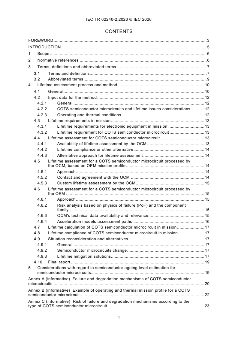
CONTENTS
FOREWORD . 3
INTRODUCTION . 5
1 Scope . 6
2 Normative references . 6
3 Terms, definitions and abbreviated terms . 7
3.1 Terms and definitions. 7
3.2 Abbreviated terms . 9
4 Lifetime assessment process and method . 10
4.1 General . 10
4.2 Input data for the method . 12
4.2.1 General . 12
4.2.2 COTS semiconductor microcircuits and lifetime issues considerations . 12
4.2.3 Operating and thermal conditions . 12
4.3 Lifetime requirements in mission . 13
4.3.1 Lifetime requirements for electronic equipment in mission . 13
4.3.2 Lifetime requirement for COTS semiconductor microcircuit . 13
4.4 Lifetime assessment for COTS semiconductor microcircuit . 13
4.4.1 Availability of lifetime assessment by the OCM . 13
4.4.2 Lifetime compliance or other alternative. 14
4.4.3 Alternative approach for lifetime assessment . 14
4.5 Lifetime assessment for a COTS semiconductor microcircuit processed by
the OCM, based on OEM mission profile . 14
4.5.1 Approach . 14
4.5.2 Contact and agreement with the OCM . 14
4.5.3 Custom lifetime assessment by the OCM . 15
4.6 Lifetime assessment for a COTS semiconductor microcircuit processed by
the OEM . 15
4.6.1 Approach . 15
4.6.2 Risk analysis based on physics of failure (PoF) and the component
family . 15
4.6.3 OCM's technical data availability and relevance. 15
4.6.4 Acceleration models assessment paths . 16
4.7 Lifetime calculation of COTS semiconductor microcircuit in mission . 17
4.8 Lifetime compliance of COTS semiconductor microcircuit in mission . 17
4.9 Situation reconsideration and alternatives . 17
4.9.1 General . 17
4.9.2 Semiconductor microcircuits change . 17
4.9.3 Lifetime mitigation solutions. 17
4.10 Final report . 19
5 Considerations with regard to semiconductor ageing level estimation for
semiconductor microcircuits. 19
Annex A (informative) Failure and degradation mechanisms of COTS semiconductor
microcircuits . 20
Annex B (informative) Example of operating and thermal mission profile for a COTS
semiconductor microcircuit. 22
Annex C (informative) Risk of failure and degradation mechanisms according to the
type of COTS semiconductor microcircuit . 23
Annex D (informative) BEOL and FEOL technological parameters . 24
Annex E (informative) Generic acceleration models . 25
Annex F (informative) Final report . 26
Bibliography . 28
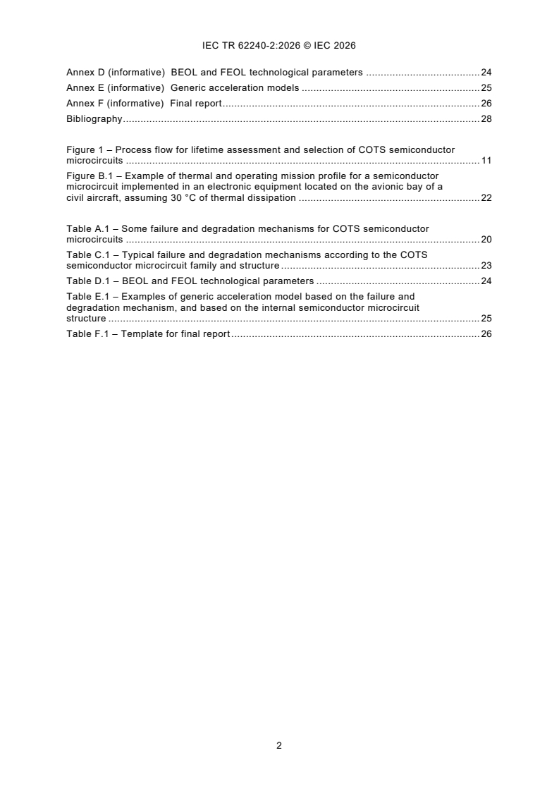
Figure 1 – Process flow for lifetime assessment and selection of COTS semiconductor
microcircuits . 11
Figure B.1 – Example of thermal and operating mission profile for a semiconductor
microcircuit implemented in an electronic equipment located on the avionic bay of a
civil aircraft, assuming 30 °C of thermal dissipation . 22
Table A.1 – Some failure and degradation mechanisms for COTS semiconductor
microcircuits . 20
Table C.1 – Typical failure and degradation mechanisms according to the COTS
semiconductor microcircuit family and structure . 23
Table D.1 – BEOL and FEOL technological parameters . 24
Table E.1 – Examples of generic acceleration model based on the failure and
degradation mechanism, and based on the internal semiconductor microcircuit
structure . 25
Table F.1 – Template for final report . 26
INTERNATIONAL ELECTROTECHNICAL COMMISSION
____________
Process management for avionics -
Electronic components capability in operation -
Part 2: Semiconductor microcircuit lifetime
FOREWORD
1) The International Electrotechnical Commission (IEC) is a worldwide organization for standardization comprising
all national electrotechnical committees (IEC National Committees). The object of IEC is to promote international
co-operation on all questions concerning standardization in the electrical and electronic fields. To this end and
in addition to other activities, IEC publishes International Standards, Technical Specifications, Technical Reports,
Publicly Available Specifications (PAS) and Guides (hereafter referred to as "IEC Publication(s)"). Their
preparation is entrusted to technical committees; any IEC National Committee interested in the subject dealt with
may participate in this preparatory work. International, governmental and non-governmental organizations liaising
with the IEC also participate in this preparation. IEC collaborates closely with the International Organization for
Standardization (ISO) in accordance with conditions determined by agreement between the two organizations.
2) The formal decisions or agreements of IEC on technical matters express, as nearly as possible, an international
consensus of opinion on the relevant subjects since each technical committee has representation from all
interested IEC National Committees.
3) IEC Publications have the form of recommendations for international use and are accepted by IEC National
Committees in that sense. While all reasonable efforts are made to ensure that the technical content of IEC
Publications is accurate, IEC cannot be held responsible for the way in which they are used or for any
misinterpretation by any end user.
4) In order to promote international uniformity, IEC National Committees undertake to apply IEC Publications
transparently to the maximum extent possible in their national and regional publications. Any divergence between
any IEC Publication and the corresponding national or regional publication shall be clearly indicated in the latter.
5) IEC itself does not provide any attestation of conformity. Independent certification bodies provide conformity
assessment services and, in some areas, access to IEC marks of conformity. IEC is not responsible for any
services carried out by independent certification bodies.
6) All users should ensure that they have the latest edition of this publication.
7) No liability shall attach to IEC or its directors, employees, servants or agents including individual experts and
members of its technical committees and IEC National Committees for any personal injury, property damage or
other damage of any nature whatsoever, whether direct or indirect, or for costs (including legal fees) and
expenses arising out of the publication, use of, or reliance upon, this IEC Publication or any other IEC
Publications.
8) Attention is drawn to the Normative references cited in this publication. Use of the referenced publications is
indispensable for the correct application of this publication.
9) IEC draws attention to the possibility that the implementation of this document may involve the use of (a)
patent(s). IEC takes no position concerning the evidence, validity or applicability of any claimed patent rights in
respect thereof. As of the date of publication of this document, IEC had not received notice of (a) patent(s), which
may be required to implement this document. However, implementers are cautioned that this may not represent
the latest information, which may be obtained from the patent database available at https://patents.iec.ch. IEC
shall not be held responsible for identifying any or all such patent rights.
IEC TR 62240-2, which is a Technical Report, has been prepared by IEC technical
committee 107: Process management for avionics. It is a Technical Report.
This second edition cancels and replaces the first edition published in 2018. This edition
constitutes a technical revision.
This edition includes the following significant technical changes with respect to the previous
edition:
a) introduction of an additional alternative path and approach where lifetime is assessed by
the original component manufacturer based on user or original equipment manufacturer
microcircuit mission profile;
b) update of Figure 1 with regard to the introduction of the additional alternative path &
approach;
c) removal of the mention of SiC & GaN technologies from the considerations in 4.2.2 as the
Scope indicates that the principles (process and method) described in this document can
be applied to all types of semiconductor technologies.
The text of this Technical Report is based on the following documents:
Draft Report on voting
107/447/DTR 107/449/RVDTR
Full information on the voting for its approval can be found in the report on voting indicated in
the above table.
The language used for the development of this Technical Report is English.
This document was drafted in accordance with ISO/IEC Directives, Part 2, and developed in
accordance with ISO/IEC Directives, Part 1 and ISO/IEC Directives, IEC Supplement, available
at www.iec.ch/members_experts/refdocs. The main document types developed by IEC are
described in greater detail at www.iec.ch/publications.
A list of all parts in the IEC 62240 series, published under the general title Process management
for avionics - Electronic components capability in operation, can be found on the IEC website.
The committee has decided that the contents of this document will remain unchanged until the
stability date indicated on the IEC website under webstore.iec.ch in the data related to the
specific document. At this date, the document will be
– reconfirmed,
– withdrawn, or
– revised.
INTRODUCTION
Electronic equipment for aerospace, defence and high performance (ADHP) applications
integrates more and more commercial off the shelf (COTS) semiconductor microcircuits. These
semiconductor microcircuits are above all designed and produced to address high volume and
low cost markets such as consumer electronics, telecommunications or microcomputers, whose
main requirements are basically cost, integration, performance and low consumption and for
which the long term reliability in severe environments (for example vibration, thermal cycling,
humidity and operating temperature) is not necessarily an imperative design criterion.
With semiconductor transistor feature size decrease, mainly from 90 nm transistor feature size,
wear-out can arise in COTS semiconductor microcircuits. For example, non-homothetic
evolution of semiconductor microcircuit bias voltage and transistor feature size scaling have led
to an increase of the electrical fields inside the semiconductor microcircuit and hence changes
in classical failure and degradation modes or mechanisms. In addition new transistor
architectures and technologies (for example fin field effect transistor (FinFET), fully depleted
silicon on insulator (FD-SOI), etc.) and new materials (for example low-k dielectrics, high-k
dielectrics, strain source/drain Si-Ge) have been introduced since the generation 90 nm, and
particularly from 45 nm and below, to overcome the scaling issues, contributing potentially to
the evolution of failure and degradation modes or mechanisms.
In this context, it might not be possible for the lifetime of new generations of COTS
semiconductor microcircuits to meet the lifetime requirements of high performance, high
reliability and long duration electronic applications (for example twenty years, thirty years or
more). As a consequence, specific reliability assessment and maintenance plans are
considered within the semiconductor microcircuit selection activities.
1 Scope
This part of IEC 62240, which is a Technical Report, focuses on original equipment
manufacturers (OEMs) using commercial off the shelf (COTS) semiconductor microcircuits for
high performance, high reliability and long duration applications. This document supports OEMs
in the preparation and maintenance of their semiconductor electronic component management
plan (ECMP).
NOTE 1 OEMs are responsible for applications reliability performance that semiconductor microcircuit lifetime can
affect; They are thus responsible for the compliance of the lifetime of the semiconductor microcircuits they use with
the lifetime requirements of the microcircuits under the applications mission conditions.
This document describes a process and a method for selecting digital semiconductor
microcircuits by ensuring that their lifetime is compatible with the requirements of aerospace,
defence and high performance (ADHP) applications (generally in connection with functional
environments). Methods and guidelines are provided to assess the long-term reliability of COTS
semiconductor microcircuits in such applications; they mainly apply during the electronic design
phase when selecting semiconductor microcircuits and assessing the application reliability.
Moreover, this document focuses on the intrinsic wear-out and the lifetime of COTS
semiconductor microcircuits processed of less than or equal to 90 nm feature size (also called
deep sub-micron (DSM) semiconductor microcircuits) and puts aside, at this time, packaging
wear-out and random failure mechanisms. In this view, physics of failure (PoF) is at the heart
of the approach.
Indeed 90 nm process node was a bend for realizing that the semiconductor wear-out and
lifetime was a concern for microcircuits processed with nodes from 90 nm and below with regard
to aerospace, defence and high performance (ADHP) mission profile.
Particularly from 45 nm and below, wear-out and lifetime remains a serious concern for long
term ADHP missions. In addition, from 28 nm, scaling is no longer a classical technology shrink
(case of planar technology for example) and different technological architectures of transistors
are introduced (for example: fin field-effect transistors (FinFETs), gate-all-around field-effect
transistors (GAAFETs)); semiconductor microcircuits in such technologies are often named
ultra-deep sub-micron (UDSM).
Although developed for COTS deep sub-micron (DSM) semiconductor microcircuits based on
silicon, the high-level approach and principles (process and method) described in this document
can apply to all types of devices technologies, for example devices processed with a gallium
nitride (GaN) technology or a silicon carbide (SiC) technology.
NOTE 2 IEC 62239-1 can assist OEMs in the creation and maintenance of ECMPs.
NOTE 3 SAE ARP6338 can also help the OEM with regard to assessment and mitigation of wear-out of life-limited
semiconductor microcircuits.
NOTE 4 With the evolution of electronic technology and semiconductor microcircuits processed of less than or equal
to 90 nm feature size, the current MIL-HDBK-217 handbook or FIDES guide become inappropriate as they are based
for the time being on the assumption that the semiconductor electronic component exhibits a constant (random)
failure rate and does not have life limits or exhibit wear-out.
Moreover, silicon itself has fundamentally very low failures in time (FIT) rates and the major failure modes are often
in the packaging (for example housing, bond wires, etc.).
Although developed for the avionics industry, this process can be applied by other industrial
sectors.
2 Normative references
There are no normative references in this document.
3 Terms, definitions and abbreviated terms
3.1 Terms and definitions
For the purposes of this document, the following terms and definitions apply.
ISO and IEC maintain terminology databases for use in standardization at the following
addresses:
– IEC Electropedia: available at https://www.electropedia.org/
– ISO Online browsing platform: available at https://www.iso.org/obp
3.1.1
acceleration model
equation for predicting time-to-fail as a function of operating stress
Note 1 to entry: An acceleration model shows how time-to-fail at a particular operating stress level can be used to
predict the equivalent time-to-fail at a different operating stress level.
Note 2 to entry: An acceleration model is associated to one failure and degradation mode or mechanism.
Acceleration models can be either defined for temperature, electrical, mechanical, environmental, or other stresses
that can affect the reliability of a device.
Note 3 to entry: An acceleration model is semi-empirical and is basically based on the physics of failure. Times are
generally derived from modeled time-to-failure distributions (lognormal, Weibull, exponential, etc.).
Note 4 to entry: The acceleration model is also defined as acceleration factor, for which the abbreviated term AF is
used.
3.1.2
cold redundancy
technique where one primary part is operational and the redundant one is in a backup mode
Note 1 to entry: The redundant part can also be called "cold" part and generally it is technically identical to the
primary part.
Note 2 to entry: The "cold" part can be non-powered or in a standby mode and it is usually called upon only on
failure of the primary part.
3.1.3
electronic equipment
functioning electronic device produced by the plan owner, which incorporates electronic
components
Note 1 to entry: End items, sub-assemblies, line-replaceable units and shop-replaceable units are examples of
electronic equipment.
[SOURCE: IEC 62239-1:2018, 3.1.20]
3.1.4
high-k dielectrics
material with a high dielectric constant "k" (as compared to silicon dioxide)
Note 1 to entry: High-k dielectrics are used in semiconductor manufacturing processes where they are usually used
to replace a silicon dioxide gate dielectric or another dielectric layer of a semiconductor microcircuit. The
implementation of high-k gate dielectrics is one of several strategies developed to allow continued scaling and
miniaturization of semiconductor microcircuits.
3.1.5
lifetime
upper bound of period of time during which the COTS semiconductor component performs a
required function without failure under stated conditions
3.1.6
low-k dielectrics
material with a small dielectric constant "k", relative to silicon dioxide
Note 1 to entry: Low-k dielectric material implementation is one of several strategies used to allow continued scaling
and miniaturization of semiconductor microcircuits.
3.1.7
NAND
Negative-AND
logic gate which produces, in digital electronics, an output that is false (0) only if all its inputs
are true (1) and an output true (1) if one or both inputs are false (0)
[SOURCE: IEC 62239-1:2018, 3.1.22]
3.1.8
NOR
Negative-OR
logic gate which produces, in digital electronics, an output that is true (1) if both the inputs are
false (0) and an output false (0) if one or both inputs are true (1)
[SOURCE: IEC 62239-1:2018, 3.1.23]
3.1.9
plan owner
original design authority responsible for all aspects of the design, functionality and reliability of
the delivered equipment in the intended application and responsible for writing and maintaining
their specific ECMP
[SOURCE: IEC 62239-1:2018, 3.1.26]
3.1.10
process node
specific semiconductor manufacturing process and its design geometry rules
Note 1 to entry: Generally, a smaller technology node means a smaller feature size, producing smaller transistors
which are both faster and more power-efficient. Historically, the name "process node" referred to a number of different
features of a transistor including the gate length as well as the first layer metal half-pitch. Most recently, due to
various marketing practices and discrepancies among foundries, the name "process node" has lost the exact meaning
it once held. Recent technology nodes below 90 nm refer purely to a specific generation of semiconductor
microcircuits made in a particular technology; they do not correspond to any gate length or half pitch. Nevertheless
the name convention has stuck and it is what the leading foundries call their nodes.
Note 2 to entry: Process node is also called technology node or simply node.
3.1.11
semiconductor microcircuit
semiconductor electronic component
electrical or electronic device that is not subject to disassembly without destruction or
impairment of design use and that utilises the properties of semiconductor materials
Note 1 to entry: It is sometimes called electronic part or electronic piece part or electronic device or electronic
component or integrated circuits. It refers to active electronic parts such as memories, microcontrollers,
microprocessors, etc.
3.1.12
wear-out
phenomenon resulting in a permanent physical degradation of a semiconductor that can be
quantified through a quasi-deterministic lifetime indicator
3.2 Abbreviated terms
ADHP aerospace, defence and high performance
AF acceleration factor
BEOL back end of the line
BTI bias temperature instability
COTS commercial off the shelf (related to semiconductor microcircuits for the
purposes of this document)
CMOS complementary metal-oxide semiconductor
DDR double data rate (memory)
DPA deprocessing analysis
DRAM dynamic random access memory
DSM deep sub-micron
ECMP electronic component management plan
EM electro-migration
EOT equivalent oxide thickness
FD-SOI fully depleted silicon on insulator
FEOL front end of the line
FeRAM ferroelectric random access memory
FinFET fin field effect transistor
FIT failures in time (number of failures that can be expected in one billion device-
hours of operation)
FPGA field programmable gate array
GAAFET gate-all-around field-effect transistors
GaN gallium nitride
Ge germanium
HCI hot carrier injection
I/O
input/output
MOSFET metal-oxide-semiconductor field-effect transistor
MRAM magnetic random access memory
NMOS N metal-oxide semiconductor
OCM original component manufacturer (related to the COTS electronic components
manufacturer)
OEM
original equipment manufacturer
PMOS P metal-oxide semiconductor
PoF physics of failure
ReRAM resistive random access memory
Si silicon
SiC silicon carbide
SDRAM synchronous dynamic random access memory
SRAM static random access memory
TDDB time dependent dielectric breakdown
TTF time to failure (or lifetime) for x % of samples
x %
UDSM ultra-deep sub-micron
4 Lifetime assessment process and method
4.1 General
The aim of the method is twofold. In a first step, this method allows the assessment and
determination of the lifetime of a COTS semiconductor microcircuit in a specific environment,
and in the second step it provides the means for the OEM to select the right COTS
semiconductor microcircuit according the electronic equipment reliability requirements.
The method is synthetized in the process flow of Figure 1.
Moreover, according to the level of information available from the OCMs or silicon foundries, or
both, four different paths can be considered:
– path and approach 1 (represented in yellow in Figure 1) where the OEM considers for its
application the lifetime assessment of the COTS semiconductor microcircuit with regard to
the lifetime specified and associated technical data provided by the OCM;
– path and approach 2 (represented in light green in Figure 1) where the lifetime is assessed
by the OCM according to the COTS semiconductor microcircuit mission profile of the OEM;
this approach requires a close collaboration between the OCM and the OEM;
– path and approach 3 (represented in orange in Figure 1) where, in the absence of lifetime
data specified by the OCM or if associated technical data are incomplete, the OEM conducts
for its application its own lifetime assessment of the COTS semiconductor microcircuit,
making a risk analysis and using the available technical data (for example, failure and
degradation mechanisms, acceleration models, raw qualification test results) provided by
the OCM;
– path and approach 4 (represented in burgundy in Figure 1) where, in case of unavailability
or irrelevancy of OCM technical data, the OEM conducts for its application its own lifetime
assessment of the COTS semiconductor microcircuit collecting potential technical data and
considering the technology of the semiconductor microcircuit (including potential
deprocessing analysis (DPA)).
Figure 1 – Process flow for lifetime assessment and selection of
COTS semiconductor microcircuits
4.2 Input data for the method
4.2.1 General
The input data for the method are as follows.
4.2.2 COTS semiconductor microcircuits and lifetime issues considerations
Wear-out effects are mainly driven by the electrical fields induced by the electrical bias of the
FEOL and BEOL stack of the semiconductor and by the increased current density with regard
to electromigration in particular. In this view, technologies nodes from 5 μm and down to the
0,1 μm were designed by the OCM to ensure constant electrical fields over the different process
node integrations. This was achieved by reducing the core bias voltages and the characteristic
dimension of the transistors with a same integration factor (around 0,3). However below 0,1
μm, this homothetic scaling of the bias core and I/O voltages was no longer possible. Therefore,
the electrical fields become more important, and the wear-out effects start to increase compared
to previous generation nodes.
NOTE Linked with scaling and semiconductor transistor feature size decrease, technological improvements on
barrier metals and alloys are regularly proposed in order to cope with the increased current density that conductors
have to carry. As the current density is the major factor that impacts electromigration, it is important to consider the
scaling effects on electromigration reliability (for more information see [5] and [17] ).
Lifetime assessment is performed on microcircuits processed with nodes from 90 nm and below
with regard to requirement and ADHP mission profile, and in particular with regard to some long
term ADHP mission profile severity (equipment mission profile with, for example, quasi
continuous operation and highly severe and very many equipment thermal cycles, etc.).
It is particularly important to consider and assess wear-out effects and lifetime for electronic
designs using COTS semiconductor microcircuits manufactured in 45 nm process nodes and
below. This includes:
– CMOS microcircuits: micro processors, microcontrollers, FPGA, SRAM;
– memories: DRAM (SDRAM, DDR series), flash memories (NAND logic gate, NOR logic
gate), MRAM, FeRAM, ReRAM.
The process node can be obtained from the original component manufacturer's datasheet or by
contacting the OCM directly.
Intrinsic failures and degradations of semiconductor microcircuits which can impact wear-out
are typically electro-migration (EM), time-dependent dielectric breakdown (TDDB), hot carrier
injection (HCI), and bias temperature instability (BTI). Annex A provides more details.
4.2.3 Operating and thermal conditions
4.2.3.1 Operating and thermal mission profiles of the electronic equipment
The OEM usually obtains this information through the electronic equipment specification,
standards, or customer requirements.
___________
Numbers in square brackets refer to the Bibliography.
4.2.3.2 Operating and thermal mission profile of COTS semiconductor microcircuit
The semiconductor microcircuit mission profile is directly derived from the electronic equipment
operation conditions (for example operating, thermal), see 4.2.3.1. In this sense, it is defined
by the OEM. The mission profile at the COTS semiconductor microcircuit level lists all stresses
applied on it during the mission life. Based on semiconductor physics of failure, the most critical
stresses identified are typically the electrical bias current/voltage and the semiconductor
microcircuit junction temperature by period of time. As an example, an operating and thermal
mission profile of a semiconductor microcircuit implemented in an avionics equipment is
provided in Annex B.
NOTE COTS semiconductor microcircuits already in use, under comparable mission profile, can provide valuable
information for risk assessment and lifetime calculation.
However, the operating and thermal mission profile of COTS semiconductor microcircuits can
potentially be reviewed in case of mitigation (see 4.9.3.1 and 4.9.3.2 related to mitigation of
stresses by mission profile).
4.3 Lifetime requirements in mission
4.3.1 Lifetime requirements for electronic equipment in mission
The OEM obtains usually this information through the electronic equipment specification or
customer requirements.
4.3.2 Lifetime requirement for COTS semiconductor microcircuit
The lifetime requirement for COTS semiconductor microcircuit in mission can be determined by
the OEM from the electronic equipment life mission.
However the lifetime requirements for COTS semiconductor microcircuits can potentially be
reviewed in case of mitigation (see 4.9.3.3 and 4.9.3.4, mitigation, respectively, by maintenance
or redundancy).
NOTE As a first step, the lifetime requirements for COTS semiconductor microcircuits can be considered the same
as the lifetime requirements for the electronic equipment.
4.4 Lifetime assessment for COTS semiconductor microcircuit
4.4.1 Availability of lifetime assessment by the OCM
If the OCM specifies and supplies a COTS semiconductor microcircuit to the OEM with the
expected lifetime under specific conditions, the OEM can check that the associated technical
data are complete.
If the OCM's technical data are complete, the OEM keeps evidence of them and can check their
relevance and acceptability (see 4.4.2).
Otherwise the OEM can consider another alternative approach for the life time assessment of
the COTS semiconductor microcircuit (see 4.4.3).
Data are considered incomplete if one of the following information is missing:
– lifetime of COTS semiconductor microcircuit for x % of failed samples;
– test parameters for which the lifetime of the COTS semiconductor microcircuit has been
estimated. Test parameters include test duration, number of tested samples, operating and
thermal conditions.
NOTE Usually this path has little chance of success as the OCM can provide lifetime based on specific conditions
which are not compatible of those of the OEM (mission profile in particular).
4.4.2 Lifetime compliance or other alternative
The OEM checks whether the COTS semiconductor microcircuit's expected lifetime under
specific conditions provided by the OCM is relevant and acceptable for the mission's lifetime
requirement.
If this lifetime is relevant and acceptable for its application, the OEM refers to 4.10 for editing
the final report and providing recommendations with regard to the selection acceptance of the
COTS semiconductor microcircuit.
If not, the OEM can envisage another initiative, either an alternative approach for lifetime
assessment (see 4.4.3) or a reconsideration of the situation (see 4.9).
4.4.3 Alternative approach for lifetime assessment
If technical data related to lifetime are not available, incomplete, not relevant or acceptable with
regard to the OEM conditions (mission profile, lifetime requirement), the OEM can consider an
alternative approach, for example:
– a lifetime assessment of the COTS semiconductor microcircuit by the OCM based on the
OEM mission profile (see 4.5); or
– a lifetime assessment of the COTS semiconductor microcircuit by itself or under its
responsibility if the service of a specialized laboratory is used for this operation (see 4.6).
4.5 Lifetime assessment for a COTS semiconductor microcircuit processed by the
OCM, based on OEM mission profile
4.5.1 Approach
In case of:
– the unavailability of lifetime assessment by the OCM, or
– incomplete, not relevant or acceptable OCM technical data with regard to the OEM
conditions (mission profile, lifetime requirement),
the OEM can potentially consider, usually with key OCMs (for example regarding key
microcircuits such as processors, memories, etc.), the possibility that OCMs assess and provide
the lifetime based on OEM mission profile (see 4.5.2).
NOTE Moreover the OEM has in most cases difficulties to obtain technical data from the OCMs, often fabless and
working with foundry companies which consider as confidential their technologies characteristics and manufacturing
processes data.
4.5.2 Contact and agreement with the OCM
To overcome the potential issues described in 4.5.1, the OEM can contact the OCM to
investigate and negotiate the possibility of a COTS semiconductor lifetime assessment by the
OCM himself, based on the OEM mission profile (see 4.5.3).
This can result usually in a non-disclosure agreement, and usually a contract, with the OCM
and potentially with the foundry company if needed and possible.
NOTE This approach cannot be generalized with all OCMs and COTS semiconductor microcircuits. Usually it is
reserved for key microcircuits and can be considered if the OEM is in a position to implement deep relationship and
discussion or cooperation with OCMs.
If an agreement is not reached, the OEM considers usually a lifetime assessment by itself (see
4.6).
4.5.3 Custom lifetime assessment by the OCM
In case of agreement between OEM and OCM, the OCM assesses the COTS semiconductor
microcircuit lifetime based on the OEM operating and thermal mission profile, and provides the
result to the OEM for compliance analysis with its lifetime requirement.
4.6 Lifetime assessment for a COTS semiconductor microcircuit processed by the
OEM
4.6.1 Approach
In the absence of lifetime specified by the OCM for a COTS semiconductor microcircuit, the
lifetime assessment can be carried out by the OEM either based on the OCM's technical data
which can be available, and according to their relevance, or through a specific activity.
A partnership between the OEM and the OCM, and sometimes the foundry, can be necessary
to obtain these technical data.
If the service of a specialized laboratory is used, the OEM keeps the responsibility of the lifetime
assessment.
4.6.2 Risk analysis based on physics of failure (PoF) and the component family
COTS semiconductor microcircuits are designed with many functional blocks and technologies
of transistors at silicon die level (for example I/O transistors, core transistors) that have their
own kinetics of degradation. Because of this, a risk analysis is performed by the OEM to make
a link between the type of semiconductor microcircuit (microprocessor, FPGA, DRAM, SRAM,
flash, etc.) and the relevant failure mechanisms (EM, TDDB BEOL, TDDB FEOL, HCI, BTI, etc.)
with the technological features involved (for example metal wire and transistor size).
The aim of this risk analysis is mainly to identify the relevant failure mechanism, putting aside
the ones which are not likely to happen with respect to the physics of failure.
An example of risk analysis by COTS semiconductor microcircuit type is given in Annex C.
NOTE The OEM considers as many acceleration model assessments as test structures identified by the risk analysis
(see 4.6.4).
4.6.3 OCM's technical data availability and relevance
Based on the semiconductor microcircuit process node qualification campaign or other specific
tests, or both, the OCM can determine, for a COTS semiconductor microcircuit, some reliability
levels at given temperatures and extract some characteristics (for example failure and
degradation mechanisms, acceleration factors) impacting the semiconductor microcircuit wear-
out and hereafter the semiconductor microcircuit lifetime.
After that the OEM conducts the following tasks:
a) Collect all the technical data (for example qualification or raw tests results obtained under
stressed conditions, failure and degradation mechanisms, acceleration models, etc.) which
can contribute to the process and extrapolate the component lifetime from the OCM's tests
conditions to the OEM's conditions as well as the failure mechanisms identified in 4.5.2.
b) Analyse their relevancy. In particular, if the raw test results are imported from product
qualification report, check whether the test conditions are relevant enough to induce the
stress corresponding to the failure mechanism described by the acceleration model. This
verification is not needed if raw test results are derived from wafer foundry qualification.
c) Identify and document, according to a) and b), a credible path:
1) acceleration models assessment with technical data from the original component
manufacturer (see 4.6.4.1);
2) acceleration models assessment conducted as a specific activity under the OEM's
responsibility (see 4.6.4.2); or
3) reconsideration of the choice of the COTS semiconductor microcircuit, selection of
another semiconductor microcircuit reference (see 4.9.2) and restart of the process from
the beginning.
NOTE As many acceleration model assessments and lifetime computations as test structures identified by the risk
analysis are considered by the OEM (see 4.6.4).
4.6.4 Acceleration models assessment paths
4.6.4.1 Acceleration models assessment by the OEM with technical data from the
OCM
If the technical data from the OCM are available and relevant (see 4.6.3), then
...
IEC TR 62240-2 ®
Edition 2.0 2026-10
TECHNICAL
REPORT
REDLINE VERSION
Process management for avionics - Electronic components capability in
operation -
Part 2: Semiconductor microcircuit lifetime
ICS 03.100.50; 31.020; 49.060 ISBN 978-2-8327-1578-9
All rights reserved. Unless otherwise specified, no part of this publication may be reproduced or utilized in any form or
by any means, electronic or mechanical, including photocopying and microfilm, without permission in writing from either
IEC or IEC's member National Committee in the country of the requester. If you have any questions about IEC copyright
or have an enquiry about obtaining additional rights to this publication, please contact the address below or your local
IEC member National Committee for further information.
IEC Secretariat Tel.: +41 22 919 02 11
3, rue de Varembé info@iec.ch
CH-1211 Geneva 20 www.iec.ch
Switzerland
About the IEC
The International Electrotechnical Commission (IEC) is the leading global organization that prepares and publishes
International Standards for all electrical, electronic and related technologies.
About IEC publications
The technical content of IEC publications is kept under constant review by the IEC. Please make sure that you have the
latest edition, a corrigendum or an amendment might have been published.
IEC publications search - IEC Products & Services Portal - products.iec.ch
webstore.iec.ch/advsearchform Discover our powerful search engine and read freely all the
The advanced search enables to find IEC publications by a publications previews, graphical symbols and the glossary.
variety of criteria (reference number, text, technical With a subscription you will always have access to up to date
committee, …). It also gives information on projects, content tailored to your needs.
replaced and withdrawn publications.
Electropedia - www.electropedia.org
The world's leading online dictionary on electrotechnology,
IEC Just Published - webstore.iec.ch/justpublished
Stay up to date on all new IEC publications. Just Published containing more than 22 500 terminological entries in English
details all new publications released. Available online and and French, with equivalent terms in 25 additional languages.
once a month by email. Also known as the International Electrotechnical Vocabulary
(IEV) online.
IEC Customer Service Centre - webstore.iec.ch/csc
If you wish to give us your feedback on this publication or
need further assistance, please contact the Customer
Service Centre: sales@iec.ch.
CONTENTS
FOREWORD . 3
INTRODUCTION . 5
1 Scope . 6
2 Normative references . 6
3 Terms, definitions and abbreviated terms . 7
3.1 Terms and definitions. 7
3.2 Abbreviated terms . 9
4 Lifetime assessment process and method . 10
4.1 General . 10
4.2 Input data for the method . 13
4.2.1 General . 13
4.2.2 COTS semiconductor microcircuits and lifetime issues considerations . 13
4.2.3 Operating and thermal conditions . 13
4.3 Lifetime requirements in mission . 14
4.3.1 Lifetime requirements for electronic equipment in mission . 14
4.3.2 Lifetime requirement for COTS semiconductor microcircuit . 14
4.4 Lifetime assessment for COTS semiconductor microcircuit based on the
OCM information . 14
4.4.1 Availability of lifetime assessment by the OCM . 14
4.4.2 Lifetime compliance or other alternative. 15
4.4.3 Alternative approach for lifetime assessment . 15
4.5 Lifetime assessment for a COTS semiconductor microcircuit processed by
the OCM, based on OEM mission profile . 15
4.5.1 Approach . 15
4.5.2 Contact and agreement with the OCM . 15
4.5.3 Custom lifetime assessment by the OCM . 16
4.6 Lifetime assessment for a COTS semiconductor microcircuit processed by
the OEM . 15
4.6.1 Approach . 16
4.6.2 Risk analysis based on physics of failure (PoF) and the component
family . 16
4.6.3 OCM's technical data availability and relevance. 16
4.6.4 Acceleration models assessment paths . 17
4.7 Lifetime calculation of COTS semiconductor microcircuit in mission . 18
4.8 Lifetime compliance of COTS semiconductor microcircuit in mission . 18
4.9 Situation reconsideration and alternatives . 18
4.9.1 General . 18
4.9.2 Semiconductor microcircuits change . 18
4.9.3 Lifetime mitigation solutions. 18
4.10 Final report . 20
5 Considerations with regard to semiconductor ageing level estimation for
semiconductor microcircuits. 20
Annex A (informative) Failure and degradation mechanisms of COTS semiconductor
microcircuits . 22
Annex B (informative) Example of operating and thermal mission profile for a COTS
semiconductor microcircuit. 24
Annex C (informative) Risk of failure and degradation mechanisms according to the
type of COTS semiconductor microcircuit . 25
Annex D (informative) BEOL and FEOL technological parameters . 26
Annex E (informative) Generic acceleration models . 27
Annex F (informative) Final report . 28
Bibliography . 30
Figure 1 – Process flow for lifetime assessment and selection of COTS semiconductor
microcircuits . 12
Figure B.1 – Example of thermal and operating mission profile for a semiconductor
microcircuit implemented in an electronic equipment located on the avionic bay of a
civil aircraft, assuming 30 °C of thermal dissipation . 24
Table A.1 – Some failure and degradation mechanisms for COTS semiconductor
microcircuits . 22
Table C.1 – Typical failure and degradation mechanisms according to the COTS
semiconductor microcircuit family and structure . 25
Table D.1 – BEOL and FEOL technological parameters . 26
Table E.1 – Examples of generic acceleration model based on the failure and
degradation mechanism, and based on the internal semiconductor microcircuit
structure . 27
Table F.1 – Template for final report . 28
INTERNATIONAL ELECTROTECHNICAL COMMISSION
____________
Process management for avionics -
Electronic components capability in operation -
Part 2: Semiconductor microcircuit lifetime
FOREWORD
1) The International Electrotechnical Commission (IEC) is a worldwide organization for standardization comprising
all national electrotechnical committees (IEC National Committees). The object of IEC is to promote international
co-operation on all questions concerning standardization in the electrical and electronic fields. To this end and
in addition to other activities, IEC publishes International Standards, Technical Specifications, Technical Reports,
Publicly Available Specifications (PAS) and Guides (hereafter referred to as "IEC Publication(s)"). Their
preparation is entrusted to technical committees; any IEC National Committee interested in the subject dealt with
may participate in this preparatory work. International, governmental and non-governmental organizations liaising
with the IEC also participate in this preparation. IEC collaborates closely with the International Organization for
Standardization (ISO) in accordance with conditions determined by agreement between the two organizations.
2) The formal decisions or agreements of IEC on technical matters express, as nearly as possible, an international
consensus of opinion on the relevant subjects since each technical committee has representation from all
interested IEC National Committees.
3) IEC Publications have the form of recommendations for international use and are accepted by IEC National
Committees in that sense. While all reasonable efforts are made to ensure that the technical content of IEC
Publications is accurate, IEC cannot be held responsible for the way in which they are used or for any
misinterpretation by any end user.
4) In order to promote international uniformity, IEC National Committees undertake to apply IEC Publications
transparently to the maximum extent possible in their national and regional publications. Any divergence between
any IEC Publication and the corresponding national or regional publication shall be clearly indicated in the latter.
5) IEC itself does not provide any attestation of conformity. Independent certification bodies provide conformity
assessment services and, in some areas, access to IEC marks of conformity. IEC is not responsible for any
services carried out by independent certification bodies.
6) All users should ensure that they have the latest edition of this publication.
7) No liability shall attach to IEC or its directors, employees, servants or agents including individual experts and
members of its technical committees and IEC National Committees for any personal injury, property damage or
other damage of any nature whatsoever, whether direct or indirect, or for costs (including legal fees) and
expenses arising out of the publication, use of, or reliance upon, this IEC Publication or any other IEC
Publications.
8) Attention is drawn to the Normative references cited in this publication. Use of the referenced publications is
indispensable for the correct application of this publication.
9) IEC draws attention to the possibility that the implementation of this document may involve the use of (a)
patent(s). IEC takes no position concerning the evidence, validity or applicability of any claimed patent rights in
respect thereof. As of the date of publication of this document, IEC had not received notice of (a) patent(s), which
may be required to implement this document. However, implementers are cautioned that this may not represent
the latest information, which may be obtained from the patent database available at https://patents.iec.ch. IEC
shall not be held responsible for identifying any or all such patent rights.
This redline version of the official IEC Standard allows the user to identify the changes made
to the previous edition IEC TR 62240-2:2018. A vertical bar appears in the margin wherever a
change has been made. Additions are in green text, deletions are in strikethrough red text.
IEC TR 62240-2, which is a Technical Report, has been prepared by IEC technical
committee 107: Process management for avionics. It is a Technical Report.
This second edition cancels and replaces the first edition published in 2018. This edition
constitutes a technical revision.
This edition includes the following significant technical changes with respect to the previous
edition:
a) introduction of an additional alternative path and approach where lifetime is assessed by
the original component manufacturer based on user or original equipment manufacturer
microcircuit mission profile;
b) update of Figure 1 with regard to the introduction of the additional alternative path &
approach;
c) removal of the mention of SiC & GaN technologies from the considerations in 4.2.2 as the
Scope indicates that the principles (process and method) described in this document can
be applied to all types of semiconductor technologies.
The text of this Technical Report is based on the following documents:
Draft Report on voting
107/447/DTR 107/449/RVDTR
Full information on the voting for its approval can be found in the report on voting indicated in
the above table.
The language used for the development of this Technical Report is English.
This document was drafted in accordance with ISO/IEC Directives, Part 2, and developed in
accordance with ISO/IEC Directives, Part 1 and ISO/IEC Directives, IEC Supplement, available
at www.iec.ch/members_experts/refdocs. The main document types developed by IEC are
described in greater detail at www.iec.ch/publications.
A list of all parts in the IEC 62240 series, published under the general title Process management
for avionics - Electronic components capability in operation, can be found on the IEC website.
The committee has decided that the contents of this document will remain unchanged until the
stability date indicated on the IEC website under webstore.iec.ch in the data related to the
specific document. At this date, the document will be
– reconfirmed,
– withdrawn, or
– revised.
INTRODUCTION
Electronic equipment for aerospace, defence and high performance (ADHP) applications
integrates more and more commercial off the shelf (COTS) semiconductor microcircuits. These
semiconductor microcircuits are above all designed and produced to address high volume and
low cost markets such as consumer electronics, telecommunications or microcomputers, whose
main requirements are basically cost, integration, performance and low consumption and for
which the long term reliability in severe environments (for example vibration, thermal cycling,
humidity and operating temperature) is not necessarily an imperative design criterion.
With semiconductor transistor feature size decrease, mainly from 90 nm transistor feature size,
wear-out can arise in COTS semiconductor microcircuits. For example, non-homothetic
evolution of semiconductor microcircuit bias voltage and transistor feature size scaling have led
to an increase of the electrical fields inside the semiconductor microcircuit and hence changes
in classical failure and degradation modes or mechanisms. In addition new transistor
architectures and technologies (for example fin field effect transistor (FinFET), fully depleted
silicon on insulator (FD-SOI), etc.) and new materials (for example low-k dielectrics, high-k
dielectrics, strain source/drain Si-Ge) have been introduced since the generation 90 nm, and
particularly from 45 nm and below, to overcome the scaling issues, contributing potentially to
the evolution of failure and degradation modes or mechanisms.
In this context, it might not be possible for the lifetime of new generations of COTS
semiconductor microcircuits may not to meet the lifetime requirements of high performance,
high reliability and long duration electronic applications (for example twenty years, thirty years
or more). As a consequence, specific reliability assessment and maintenance plans are
considered within the semiconductor microcircuit selection activities.
1 Scope
This part of IEC 62240, which is a Technical Report, focuses on original equipment
manufacturers (OEMs) using commercial off the shelf (COTS) semiconductor microcircuits for
high performance, high reliability and long duration applications. This document supports OEMs
in the preparation and maintenance of their semiconductor electronic component management
plan (ECMP).
NOTE 1 OEMs are responsible for applications reliability performance that semiconductor microcircuit lifetime can
affect; They are thus responsible for the compliance of the lifetime of the semiconductor microcircuits they use with
the lifetime requirements of the microcircuits under the applications mission conditions.
This document describes a process and a method for selecting digital semiconductor
microcircuits by ensuring that their lifetime is compatible with the requirements of aerospace,
defence and high performance (ADHP) applications (generally in connection with functional
environments). Methods and guidelines are provided to assess the long-term reliability of COTS
semiconductor microcircuits in such applications; they mainly apply during the electronic design
phase when selecting semiconductor microcircuits and assessing the application reliability.
Moreover, this document focuses on the intrinsic wear-out and the lifetime of COTS
semiconductor microcircuits processed of less than or equal to 90 nm feature size (also called
deep sub-micron (DSM) semiconductor microcircuits) and puts aside, at this time, packaging
wear-out and random failure mechanisms. In this view, physics of failure (PoF) is at the heart
of the approach.
Indeed 90 nm process node was a bend for realizing that the semiconductor wear-out and
lifetime was a concern for microcircuits processed with nodes from 90 nm and below with regard
to aerospace, defence and high performance (ADHP) mission profile.
Particularly from 45 nm and below, wear-out and lifetime remains a serious concern for long
term ADHP missions. In addition, from 28 nm, scaling is no longer a classical technology shrink
(case of planar technology for example) and different technological architectures of transistors
are introduced (for example: fin field-effect transistors (FinFETs), gate-all-around field-effect
transistors (GAAFETs)); semiconductor microcircuits in such technologies are often named
ultra-deep sub-micron (UDSM).
Although developed for COTS deep sub-micron (DSM) semiconductor microcircuits based on
silicon, the high-level approach and principles (process and method) described in this document
can apply to all types of devices technologies, for example devices processed with a gallium
nitride (GaN) technology or a silicon carbide (SiC) technology.
NOTE 2 IEC 62239-1 can assist OEMs in the creation and maintenance of ECMPs.
NOTE 3 SAE ARP6338 can also help the OEM with regard to assessment and mitigation of wear-out of life-limited
semiconductor microcircuits.
NOTE 4 With the evolution of electronic technology and semiconductor microcircuits processed of less than or equal
to 90 nm feature size, the current MIL-HDBK-217 handbook or FIDES guide become inappropriate as they are based
for the time being on the assumption that the semiconductor electronic component exhibits a constant (random)
failure rate and does not have life limits or exhibit wear-out.
Moreover, silicon itself has fundamentally very low failures in time (FIT) rates and the major failure modes are often
in the packaging (for example housing, bond wires, etc.).
Although developed for the avionics industry, this process can be applied by other industrial
sectors.
2 Normative references
There are no normative references in this document.
3 Terms, definitions and abbreviated terms
3.1 Terms and definitions
For the purposes of this document, the following terms and definitions apply.
ISO and IEC maintain terminology databases for use in standardization at the following
addresses:
– IEC Electropedia: available at https://www.electropedia.org/
– ISO Online browsing platform: available at https://www.iso.org/obp
3.1.1
acceleration model
equation for predicting time-to-fail as a function of operating stress
Note 1 to entry: An acceleration model shows how time-to-fail at a particular operating stress level can be used to
predict the equivalent time-to-fail at a different operating stress level.
Note 2 to entry: An acceleration model is associated to one failure and degradation mode or mechanism.
Acceleration models can be either defined for temperature, electrical, mechanical, environmental, or other stresses
that can affect the reliability of a device.
Note 3 to entry: An acceleration model is semi-empirical and is basically based on the physics of failure. Times are
generally derived from modeled time-to-failure distributions (lognormal, Weibull, exponential, etc.).
Note 4 to entry: The acceleration model is also defined as acceleration factor, for which the abbreviated term AF is
used.
3.1.2
Bi-CMOS
bipolar CMOS
technology integrating two separate semiconductor technologies, bipolar junction transistor and
CMOS transistor, in a single electronic component
3.1.2
cold redundancy
technique where one primary part is operational and the redundant one is in a backup mode
Note 1 to entry: The redundant part can also be called "cold" part and generally it is technically identical to the
primary part.
Note 2 to entry: The "cold" part can be non-powered or in a standby mode and it is usually called upon only on
failure of the primary part.
3.1.3
electronic equipment
functioning electronic device produced by the plan owner, which incorporates electronic
components
Note 1 to entry: End items, sub-assemblies, line-replaceable units and shop-replaceable units are examples of
electronic equipment.
[SOURCE: IEC 62239-1:2018, 3.1.20]
3.1.4
high-k dielectrics
material with a high dielectric constant "k" (as compared to silicon dioxide)
Note 1 to entry: High-k dielectrics are used in semiconductor manufacturing processes where they are usually used
to replace a silicon dioxide gate dielectric or another dielectric layer of a semiconductor microcircuit. The
implementation of high-k gate dielectrics is one of several strategies developed to allow continued scaling and
miniaturization of semiconductor microcircuits.
3.1.5
lifetime
upper bound of period of time during which the COTS semiconductor component performs a
required function without failure under stated conditions
3.1.6
low-k dielectrics
material with a small dielectric constant "k", relative to silicon dioxide
Note 1 to entry: Low-k dielectric material implementation is one of several strategies used to allow continued scaling
and miniaturization of semiconductor microcircuits.
3.1.7
NAND
Negative-AND
logic gate which produces, in digital electronics, an output that is false (0) only if all its inputs
are true (1) and an output true (1) if one or both inputs are false (0)
[SOURCE: IEC 62239-1:2018, 3.1.22]
3.1.8
NOR
Negative-OR
logic gate which produces, in digital electronics, an output that is true (1) if both the inputs are
false (0) and an output false (0) if one or both inputs are true (1)
[SOURCE: IEC 62239-1:2018, 3.1.23]
3.1.9
plan owner
original design authority responsible for all aspects of the design, functionality and reliability of
the delivered equipment in the intended application and responsible for writing and maintaining
their specific ECMP
[SOURCE: IEC 62239-1:2018, 3.1.26]
3.1.10
process node
specific semiconductor manufacturing process and its design geometry rules
Note 1 to entry: Generally, a smaller technology node means a smaller feature size, producing smaller transistors
which are both faster and more power-efficient. Historically, the name "process node" referred to a number of different
features of a transistor including the gate length as well as the first layer metal half-pitch. Most recently, due to
various marketing practices and discrepancies among foundries, the name "process node" has lost the exact meaning
it once held. Recent technology nodes below 90 nm refer purely to a specific generation of semiconductor
microcircuits made in a particular technology; they do not correspond to any gate length or half pitch. Nevertheless
the name convention has stuck and it is what the leading foundries call their nodes.
Note 2 to entry: Process node is also called technology node or simply node.
3.1.11
semiconductor microcircuit
semiconductor electronic component
electrical or electronic device that is not subject to disassembly without destruction or
impairment of design use and that utilises the properties of semiconductor materials
Note 1 to entry: It is sometimes called electronic part or electronic piece part or electronic device or electronic
component or integrated circuits. It refers to active electronic parts such as memories, microcontrollers,
microprocessors, etc.
3.1.12
wear-out
phenomenon resulting in a permanent physical degradation of a semiconductor that can be
quantified through a quasi-deterministic lifetime indicator
3.2 Abbreviated terms
ADHP aerospace, defence and high performance
AF acceleration factor
BEOL back end of the line
BTI bias temperature instability
COTS commercial off the shelf (related to semiconductor microcircuits for the
purposes of this document)
CMOS complementary metal-oxide semiconductor
DDR double data rate (memory)
DPA deprocessing analysis
DRAM dynamic random access memory
DSM deep sub-micron
ECMP electronic component management plan
EM electro-migration
EOT equivalent oxide thickness
FD-SOI fully depleted silicon on insulator
FEOL front end of the line
FeRAM ferroelectric random access memory
FinFET fin field effect transistor
FIT failures in time (number of failures that can be expected in one billion device-
hours of operation)
FPGA field programmable gate array
GAAFET gate-all-around field-effect transistors
GaN gallium nitride
Ge germanium
HCI hot carrier injection
I/O input/output
MOSFET metal-oxide-semiconductor field-effect transistor
MRAM
magnetic random access memory
NMOS N metal-oxide semiconductor
OCM original component manufacturer (related to the COTS electronic components
manufacturer)
OEM original equipment manufacturer
PMOS P metal-oxide semiconductor
PoF physics of failure
ReRAM resistive random access memory
Si silicon
SiC silicon carbide
SDRAM synchronous dynamic random access memory
SRAM static random access memory
TDDB time dependent dielectric breakdown
TTF time to failure (or lifetime) for x % of samples
x %
UDSM ultra-deep sub-micron
4 Lifetime assessment process and method
4.1 General
The aim of the method is twofold. In a first step, this method allows the assessment and
determination of the lifetime of a COTS semiconductor microcircuit in a specific environment,
and in the second step it provides the means for the OEM to select the right COTS
semiconductor microcircuit according the electronic equipment reliability requirements.
The method is synthetized in the process flow of Figure 1.
Moreover, according to the level of information available from the OCMs or silicon foundries, or
both, three four different paths can be considered:
– path and approach 1 (represented in yellow in Figure 1) where the OEM considers for its
application the lifetime assessment of the COTS semiconductor microcircuit with regard to
the lifetime specified and associated technical data provided by the OCM;
– path and approach 2 (represented in light green in Figure 1) where the lifetime is assessed
by the OCM according to the COTS semiconductor microcircuit mission profile of the OEM;
this approach requires a close collaboration between the OCM and the OEM;
– path and approach 23 (represented in orange in Figure 1) where, in the absence of lifetime
data specified by the OCM or if associated technical data are incomplete, the OEM conducts
for its application its own lifetime assessment of the COTS semiconductor microcircuit,
making a risk analysis and using the available technical data (for example, failure and
degradation mechanisms, acceleration models, raw qualification test results) provided by
the OCM;
– path and approach 34 (represented in burgundy in Figure 1) where, in case of unavailability
or irrelevancy of OCM technical data, the OEM conducts for its application its own lifetime
assessment of the COTS semiconductor microcircuit collecting potential technical data and
considering the technology of the semiconductor microcircuit (including potential
deprocessing analysis (DPA)).
Figure 1 – Process flow for lifetime assessment and selection of
COTS semiconductor microcircuits
4.2 Input data for the method
4.2.1 General
The input data for the method are as follows.
4.2.2 COTS semiconductor microcircuits and lifetime issues considerations
Wear-out effects are mainly driven by the electrical fields induced by the electrical bias of the
FEOL and BEOL stack of the semiconductor and by the increased current density with regard
to electromigration in particular. In this view, technologies nodes from 5 μm and down to the
0,1 μm were designed by the OCM to ensure constant electrical fields over the different process
node integrations. This was achieved by reducing the core bias voltages and the characteristic
dimension of the transistors with a same integration factor (around 0,3). However below 0,1
μm, this homothetic scaling of the bias core and I/O voltages was no longer possible. Therefore,
the electrical fields become more important, and the wear-out effects start to increase compared
to previous generation nodes.
NOTE Linked with scaling and semiconductor transistor feature size decrease, technological improvements on
barrier metals and alloys are regularly proposed in order to cope with the increased current density that conductors
have to carry. As the current density is the major factor that impacts electromigration, it is important to consider the
scaling effects on electromigration reliability (for more information see [5] and [17] ).
Lifetime assessment is performed on microcircuits processed with nodes from 90 nm and below
with regard to requirement and ADHP mission profile, and in particular with regard to some long
term ADHP mission profile severity (equipment mission profile with, for example, quasi
continuous operation and highly severe and very many equipment thermal cycles, etc.).
It is particularly important to consider and assess wear-out effects and lifetime considerations
need to be taken into account for electronic designs using COTS semiconductor microcircuits
manufactured in 90 45 nm process nodes and below. This includes digital COTS semiconductor
microcircuits such as SRAM, DRAM (SDRAM, DDR series), flash memories (NOR logic gate,
NAND logic gate), MRAM, microcontrollers, microprocessors and FPGA. Analog or Bi-CMOS
electronic components can also be concerned and a similar approach can be used.
This includes:
– CMOS microcircuits: micro processors, microcontrollers, FPGA, SRAM;
– memories: DRAM (SDRAM, DDR series), flash memories (NAND logic gate, NOR logic
gate), MRAM, FeRAM, ReRAM.
The process node can be obtained from the original component manufacturer's datasheet or
indicated on the part number marking or by contacting the OCM directly.
Intrinsic failures and degradations of semiconductor microcircuits which can impact wear-out
are typically electro-migration (EM), time-dependent dielectric breakdown (TDDB), hot carrier
injection (HCI), and bias temperature instability (BTI). Annex A provides more details.
4.2.3 Operating and thermal conditions
4.2.3.1 Operating and thermal mission profiles of the electronic equipment
The OEM usually obtains this information through the electronic equipment specification,
standards, or customer requirements.
___________
Numbers in square brackets refer to the Bibliography.
4.2.3.2 Operating and thermal mission profile of COTS semiconductor microcircuit
The semiconductor microcircuit mission profile is directly derived from the electronic equipment
operation conditions (for example operating, thermal), see 4.2.3.1. In this sense, it is defined
by the OEM. The mission profile at the COTS semiconductor microcircuit level lists all stresses
applied on it during the mission life. Based on semiconductor physics of failure, the most critical
stresses identified are typically the electrical bias current/voltage and the semiconductor
microcircuit junction temperature by period of time. As an example, an operating and thermal
mission profile of a semiconductor microcircuit implemented in an avionics equipment is
provided in Annex B.
NOTE COTS semiconductor microcircuits already in use, under comparable mission profile, can provide valuable
information for risk assessment and lifetime calculation.
However, the operating and thermal mission profile of COTS semiconductor microcircuits can
potentially be reviewed in case of mitigation (see 4.9.3.1 and 4.9.3.2 related to mitigation of
stresses by mission profile).
4.3 Lifetime requirements in mission
4.3.1 Lifetime requirements for electronic equipment in mission
The OEM obtains usually this information through the electronic equipment specification or
customer requirements.
4.3.2 Lifetime requirement for COTS semiconductor microcircuit
The lifetime requirement for COTS semiconductor microcircuit in mission can be determined by
the OEM from the electronic equipment life mission.
However the lifetime requirements for COTS semiconductor microcircuits can potentially be
reviewed in case of mitigation (see 4.9.3.3 and 4.9.3.4, mitigation, respectively, by maintenance
or redundancy).
NOTE As a first step, the lifetime requirements for COTS semiconductor microcircuits can be considered the same
as the lifetime requirements for the electronic equipment.
4.4 Lifetime assessment for COTS semiconductor microcircuit based on the OCM
information
4.4.1 Availability of lifetime assessment by the OCM
If the OCM specifies and supplies a COTS semiconductor microcircuit to the OEM with the
expected lifetime under specific conditions, the OEM can check that the associated technical
data are complete.
If the OCM's technical data are complete, the OEM keeps evidence of them and can check their
relevance and acceptability (see 4.4.2).
Otherwise the OEM can itself assess consider another alternative approach for the life time
assessment of the COTS semiconductor microcircuit (see 4.4.3).
Data are considered incomplete if one of the following information is missing:
– lifetime of COTS semiconductor microcircuit for x % of failed samples;
– test parameters for which the lifetime of the COTS semiconductor microcircuit has been
estimated. Test parameters include test duration, number of tested samples, operating and
thermal conditions.
NOTE Usually this path has little chance of success as the OCM can provide lifetime based on specific conditions
which are not compatible of those of the OEM (mission profile in particular).
4.4.2 Lifetime compliance or other alternative
The OEM checks whether the COTS semiconductor microcircuit's expected lifetime under
specific conditions provided by the OCM is relevant and acceptable for both the OEM’s
operating and thermal mission profiles and the mission's lifetime requirement.
If this lifetime is relevant and acceptable for its application, the OEM refers to 4.10 for editing
the final report and providing recommendations with regard to the selection acceptance of the
COTS semiconductor microcircuit.
If not, the OEM can reconsider envisage another initiative, either an alternative approach for
lifetime assessment (see 4.4.3) or a reconsideration of the situation (see 4.9).
4.4.3 Alternative approach for lifetime assessment
If technical data related to lifetime are not available, incomplete, not relevant or acceptable with
regard to the OEM conditions (mission profile, lifetime requirement), the OEM can consider an
alternative approach, for example:
– a lifetime assessment of the COTS semiconductor microcircuit by the OCM based on the
OEM mission profile (see 4.5); or
– a lifetime assessment of the COTS semiconductor microcircuit by itself or under its
responsibility if the service of a specialized laboratory is used for this operation (see 4.6).
4.5 Lifetime assessment for a COTS semiconductor microcircuit processed by the
OCM, based on OEM mission profile
4.5.1 Approach
In case of:
– the unavailability of lifetime assessment by the OCM, or
– incomplete, not relevant or acceptable OCM technical data with regard to the OEM
conditions (mission profile, lifetime requirement),
the OEM can potentially consider, usually with key OCMs (for example regarding key
microcircuits such as processors, memories, etc.), the possibility that OCMs assess and provide
the lifetime based on OEM mission profile (see 4.5.2).
NOTE Moreover the OEM has in most cases difficulties to obtain technical data from the OCMs, often fabless and
working with foundry companies which consider as confidential their technologies characteristics and manufacturing
processes data.
4.5.2 Contact and agreement with the OCM
To overcome the potential issues described in 4.5.1, the OEM can contact the OCM to
investigate and negotiate the possibility of a COTS semiconductor lifetime assessment by the
OCM himself, based on the OEM mission profile (see 4.5.3).
This can result usually in a non-disclosure agreement, and usually a contract, with the OCM
and potentially with the foundry company if needed and possible.
NOTE This approach cannot be generalized with all OCMs and COTS semiconductor microcircuits. Usually it is
reserved for key microcircuits and can be considered if the OEM is in a position to implement deep relationship and
discussion or cooperation with OCMs.
If an agreement is not reached, the OEM considers usually a lifetime assessment by itself
(see 4.6).
4.5.3 Custom lifetime assessment by the OCM
In case of agreement between OEM and OCM, the OCM assesses the COTS semiconductor
microcircuit lifetime based on the OEM operating and thermal mission profile, and provides the
result to the OEM for compliance analysis with its lifetime requirement.
4.6 Lifetime assessment for a COTS semiconductor microcircuit processed by the
OEM
4.6.1 Approach
In the absence of lifetime specified by the OCM for a COTS semiconductor microcircuit, the
lifetime assessment can be carried out by the OEM either based on the OCM's technical data
which can be available, and according to their relevance, or through a specific activity.
A partnership between the OEM and the OCM, and sometimes the foundry, can be necessary
to obtain these technical data.
If the service of a specialized laboratory is used, the OEM keeps the responsibility of the lifetime
assessment.
4.6.2 Risk analysis based on physics of failure (PoF) and the component family
COTS semiconductor microcircuits are designed with many functional blocks and technologies
of transistors at silicon die level (for example I/O transistors, core transistors) that have their
own kinetics of degradation. Because of this, a risk analysis is performed by the OEM to make
a link between the type of semiconductor microcircuit (microprocessor, FPGA, DRAM, SRAM,
flash, etc.) and the relevant failure mechanisms (EM, TDDB BEOL, TDDB FEOL, HCI, BTI, etc.)
with the technological features involved (for example metal wire and transistor size).
The aim of this risk analysis is mainly to identify the relevant failure mechanism, putting aside
the ones which are not likely to happen with respect to the physics of failure.
An example of risk analysis by COTS semiconductor microcircuit type is given in Annex C.
NOTE The OEM considers as many acceleration model assessments as test structures identified by the risk analysis
(see 4.6.4).
4.6.3 OCM's technical data availability and relevance
Based on the semiconductor microcircuit process node qualification campaign or other specific
tests, or both, the OCM can determine, for a COTS semiconductor microcircuit, some reliability
levels at given temperatures and extract some characteristics (for example failure and
degradation mechanisms, acceleration factors) impacting the semiconductor microcircuit wear-
out and hereafter the semiconductor microcircuit lifetime.
After that the OEM conducts the following tasks:
a) Collect all the technical data (for example qualification and/or raw tests results obtained
under stressed conditions, failure and degradation mechanisms, acceleration models, etc.)
which can contribute to the process and extrapolate the component lifetime from the OCM's
tests conditions to the OEM's conditions as well as the failure mechanisms identified in
4.5.2.
b) Analyse their relevancy. In particular, if the raw test results are i
...