ASTM F1393-92(1997)
(Test Method)Standard Test Method for Determining Net Carrier Density in Silicon Wafers by Miller Feedback Profiler Measurements With a Mercury Probe
Standard Test Method for Determining Net Carrier Density in Silicon Wafers by Miller Feedback Profiler Measurements With a Mercury Probe
SCOPE
1.1 This test method covers the measurement of net carrier density and net carrier density profiles in epitaxial and polished bulk silicon wafers in the range from about 4 X 10 13 to about 8 X 10 16 carriers/cm (resistivity range from about 0.1 to about 100 [omega]-cm in n-type wafers and from about 0.24 to about 330 [omega]-cm in p-type wafers).
1.2 This test method requires the formation of a Schottky barrier diode with a mercury probe contact to an epitaxial or polished wafer surface. Chemical treatment of the silicon surface may be required to produce a reliable Schottky barrier diode. (1) The surface treatment chemistries are different for n- and p-type wafers. This test method is sometimes considered destructive due to the possibility of contamination from the Schottky contact formed on the wafer surface; however, repetitive measurements may be made on the same test specimen.
1.3 This test method may be applied to epitaxial layers on the same or opposite conductivity type substrate. This test method includes descriptions of fixtures for measuring substrates with or without an insulating backseal layer.
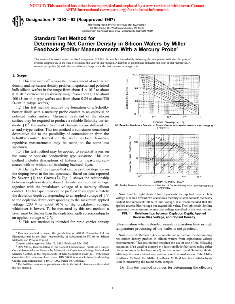
1.4 The depth of the region that can be profiled depends on the doping level in the test specimen. Based on data reported by Severin (1) and Grove (2), Fig. 1 shows the relationship between depletion depth, dopant density, and applied voltage together with the breakdown voltage of a mercury silicon contact. The test specimen can be profiled from approximately the depletion depth corresponding to an applied voltage of 1 V to the depletion depth corresponding to the maximum applied voltage (200 V or about 80% of the breakdown voltage, whichever is lower). To be measured by this test method, a layer must be thicker than the depletion depth corresponding to an applied voltage of 2 V.
1.5 This test method is intended for rapid carrier density determination when extended sample preparation time or high temperature processing of the wafer is not practical. Note 1-Test Method F419 is an alternative method for determining net carrier density profiles in silicon wafers from capacitance-voltage measurements. This test method requires the use of one of the following structures: (1) a gated or ungated p-n junction diode fabricated using either planar or mesa technology or (2) an evaporated metal Schottky diode. Although this test method was written prior to consideration of the Miller Feedback Method, the Miller Feedback Method has been satisfactorily used in measuring the round robin samples.
1.6 This test method provides for determining the effective area of the mercury probe contact using polished bulk reference wafers that have been measured for resistivity at 23°C in accordance with Test Method F84 or Test Method F673. This test method also includes procedures for calibration of the apparatus. Note 2-An alternative method of determining the effective area of the mercury probe contact that involves the use of reference wafers whose net carrier density has been measured using fabricated mesa or planar p-n junction diodes or evaporated Schottky diodes is not included Note-The light dashed line represents the applied reverse bias voltage at which breakdown occurs in a mercury silicon contact; the heavy dashed line represents 80% of this voltage, it is recommended that the applied reverse bias voltage not exceed this value. The light chain-dot line represents the maximum reverse bias voltage specified in this test method. FIG. 1% Relationships between Depletion Depth, Applied Reverse Bias Voltage, and Dopant Density in this test method but may be used if agreed upon by the parties to the test.
1.7 This standard does not purport to address all of the safety problems, if any, associated with its use. It is the responsibility of the user of this standard to establish appropriate safety and health practices and determine the applicability of regulatory limitations prior to use. Specific hazard stateme...
General Information
Relations
Standards Content (Sample)
NOTICE: This standard has either been superseded and replaced by a new version or withdrawn. Contact
ASTM International (www.astm.org) for the latest information.
Designation: F 1393 – 92 (Reapproved 1997)
AMERICAN SOCIETY FOR TESTING AND MATERIALS
100 Barr Harbor Dr., West Conshohocken, PA 19428
Reprinted from the Annual Book of ASTM Standards. Copyright ASTM
Standard Test Method for
Determining Net Carrier Density in Silicon Wafers by Miller
1
Feedback Profiler Measurements With a Mercury Probe
This standard is issued under the fixed designation F 1393; the number immediately following the designation indicates the year of
original adoption or, in the case of revision, the year of last revision. A number in parentheses indicates the year of last reapproval. A
superscript epsilon (e) indicates an editorial change since the last revision or reapproval.
1. Scope
2
1.1 This test method covers the measurement of net carrier
density and net carrier density profiles in epitaxial and polished
13
bulk silicon wafers in the range from about 4 3 10 to about
16
8 3 10 carriers/cm (resistivity range from about 0.1 to about
100 V-cm in n-type wafers and from about 0.24 to about 330
V-cm in p-type wafers).
1.2 This test method requires the formation of a Schottky
barrier diode with a mercury probe contact to an epitaxial or
polished wafer surface. Chemical treatment of the silicon
surface may be required to produce a reliable Schottky barrier
3
diode. (1) The surface treatment chemistries are different for
n- and p-type wafers. This test method is sometimes considered
destructive due to the possibility of contamination from the
Schottky contact formed on the wafer surface; however,
repetitive measurements may be made on the same test
specimen.
1.3 This test method may be applied to epitaxial layers on
the same or opposite conductivity type substrate. This test
method includes descriptions of fixtures for measuring sub-
strates with or without an insulating backseal layer.
1.4 The depth of the region that can be profiled depends on
the doping level in the test specimen. Based on data reported
by Severin (1) and Grove (2), Fig. 1 shows the relationship
between depletion depth, dopant density, and applied voltage
together with the breakdown voltage of a mercury silicon
contact. The test specimen can be profiled from approximately
NOTE 1—The light dashed line represents the applied reverse bias
the depletion depth corresponding to an applied voltage of 1 V
voltage at which breakdown occurs in a mercury silicon contact; the heavy
to the depletion depth corresponding to the maximum applied
dashed line represents 80 % of this voltage, it is recommended that the
voltage (200 V or about 80 % of the breakdown voltage,
applied reverse bias voltage not exceed this value. The light chain-dot line
whichever is lower). To be measured by this test method, a
represents the maximum reverse bias voltage specified in this test method.
layer must be thicker than the depletion depth corresponding to FIG. 1 Relationships between Depletion Depth, Applied
Reverse Bias Voltage, and Dopant Density
an applied voltage of 2 V.
1.5 This test method is intended for rapid carrier density
determination when extended sample preparation time or high
temperature processing of the wafer is not practical.
1
This test method is under the jurisdiction of ASTM Committee F-1 on
NOTE 1—Test Method F 419 is an alternative method for determining
Electronics and its the direct responsibility of Subcommittee F01.06 on Silicon
net carrier density profiles in silicon wafers from capacitance-voltage
Materials and Process Control.
measurements. This test method requires the use of one of the following
Current edition approved May 15, 1992. Published July 1992.
2
structures: (1) a gated or ungated p-n junction diode fabricated using either
DIN 50439, Determination of the Dopant Concentration Profile of a Single
Crystal Semiconductor Material by Means of the Capacitance-Voltage Method and planar or mesa technology or (2) an evaporated metal Schottky diode.
Mercury Contact, is the responsibility of DIN Committee NMP 221, with which
Although this test method was written prior to consideration of the Miller
Committee F-1 maintains close liaison. DIN 50439 is available from Beuth Verlag
Feedback Method, the Miller Feedback Method has been satisfactorily
GmbH, Burggrafenstrasse 4-10, D-1000, Berlin 30, Germany.
used in measuring the round robin samples.
3
The boldface numbers in parenthesis refer to the list of references at the end of
this test method. 1.6 This test method provides for determining the effective
1
---------------------- Page: 1 ----------------------
NOTICE:¬This¬standard¬has¬either¬been¬superceded¬and¬replaced¬by¬a¬new¬version¬or¬discontinued.¬
Contact¬ASTM¬International¬(www.astm.org)¬for¬the¬latest¬information.¬
F 1393
area of the mercury probe contact using polished bulk refer- contact does not result in excessive series resistance as
ence wafers that have bee
...


Questions, Comments and Discussion
Ask us and Technical Secretary will try to provide an answer. You can facilitate discussion about the standard in here.