

prEN IEC 61191-10-2:2026
(Main)Circuit board assemblies - Part 10-2 : Guideline for Establishing Bonding Parameters in Laser-Assisted Bonding between Semiconductor Chip and Substrate
General Information
- Abstract
- Status
- Not Published
- Publication Date
- 09-Mar-2028
- Technical Committee
- CLC/SR 91 - Electronics assembly technology
- Current Stage
- 4020 - Enquiry circulated - Enquiry
- Start Date
- 21-Aug-2026
- Due Date
- 29-May-2026
- Completion Date
- 21-Aug-2026

Overview
prEN IEC 61191-10-2:2026, developed by CLC, sets out a guideline for establishing bonding parameters in laser-assisted bonding (LAB) between semiconductor chips and substrates. This document provides practical recommendations for setting key parameters-such as laser energy, time, and temperature profiles-for reliable bonds in advanced circuit board assemblies, specifically in flip-chip packaging and similar applications.
The increased miniaturization and complexity of electronic components necessitate precision processes like LAB. Unlike conventional mass reflow, LAB enables targeted, rapid heating for soldering chips with minimal substrate distortion. Establishing appropriate bonding parameters is vital for ensuring optimal electrical connectivity, mechanical stability, and long-term reliability in electronic devices.
Key Topics
Laser-Assisted Bonding (LAB):
A process where a semiconductor chip is bonded to a substrate using focused laser energy. LAB allows localized heating, reducing warpage and improving throughput for high-density assemblies.Bonding Parameters:
Guidelines for determining the appropriate laser power, duration, bonding temperature, and pressure to achieve consistent, robust solder joints.Materials & Equipment:
The standard outlines relevant materials such as solder balls, non-conductive adhesives (NCA), and devices like near-infrared diode lasers, thermocouples, and homogenizers to ensure uniform laser delivery.Temperature Profiling:
Emphasis on measuring time–temperature profiles during bonding to optimize solder reflow and reduce defects, such as voids and misalignments.Testing and Inspection:
Use of X-ray and optical inspections to assess void content, joint alignment, and electrical clearance in soldered connections, aligned with IPC and IEC criteria for BGA (Ball Grid Array) assemblies.
Applications
prEN IEC 61191-10-2:2026 is highly relevant for manufacturers and engineers involved in advanced electronics assembly, particularly in the following sectors:
Flip-Chip Packaging:
Used extensively in microelectronics where space constraints and thermal management are critical. The guideline helps achieve consistent bonding needed for reliability in consumer electronics, computing, and telecommunications.LED and Solar Cell Bonding:
LAB supports high-precision, low-thermal-stress bonding for optoelectronics and renewable energy sectors, where component sensitivity is a concern.MEMS Hermetic Sealing:
For micro-electromechanical systems requiring hermeticity, LAB offers an efficient solution for joining components with minimal risk of heat-induced warpage or structural failures.Automotive Electronic Control Units:
The recommendations contribute to achieving robust solder joints for high-reliability automotive applications, supporting best practices for void control and component alignment.
Related Standards
To ensure best practices and interoperability in electronic assembly, the following standards provide complementary guidance:
IEC 61191-6:
Covers evaluation criteria for voids in soldered joints of BGA and LGA, along with measurement methods.IEC TR 61191-8:
Offers best practices for voiding in solder joints for automotive electronic control units.IPC-A-610:
Globally recognized standard for the acceptability of electronic assemblies, including detailed inspection requirements for soldered connections.
Practical Value
By adhering to prEN IEC 61191-10-2:2026, organizations can:
- Achieve higher production yields through optimized bonding parameters,
- Reduce incidence of defects such as voids, misalignment, and insufficient bonding,
- Improve product reliability for mission-critical applications in demanding markets like automotive, telecommunications, and renewable energy,
- Streamline processes for new product introduction involving densely packed and miniaturized electronic assemblies.
Embracing laser-assisted bonding guidelines empowers manufacturers to stay at the forefront of electronics assembly technology, ensuring their products meet global quality and dependability benchmarks.
Frequently Asked Questions
prEN IEC 61191-10-2:2026 is a draft published by CLC. Its full title is "Circuit board assemblies - Part 10-2 : Guideline for Establishing Bonding Parameters in Laser-Assisted Bonding between Semiconductor Chip and Substrate". This standard covers: Circuit board assemblies - Part 10-2 : Guideline for Establishing Bonding Parameters in Laser-Assisted Bonding between Semiconductor Chip and Substrate
Circuit board assemblies - Part 10-2 : Guideline for Establishing Bonding Parameters in Laser-Assisted Bonding between Semiconductor Chip and Substrate
prEN IEC 61191-10-2:2026 is classified under the following ICS (International Classification for Standards) categories: 31.180 - Printed circuits and boards; 31.190 - Electronic component assemblies. The ICS classification helps identify the subject area and facilitates finding related standards.
prEN IEC 61191-10-2:2026 is available in PDF format for immediate download after purchase. The document can be added to your cart and obtained through the secure checkout process. Digital delivery ensures instant access to the complete standard document.
Standards Content (Sample)
SLOVENSKI STANDARD
01-oktober-2026
Sestavi plošč tiskanih vezi - 10-2.del: Smernice za določanje parametrov spajanja
pri lasersko podprtem spajanju med polprevodniškim čipom in substratom
Circuit board assemblies - Part 10-2 : Guideline for Establishing Bonding Parameters in
Laser-Assisted Bonding between Semiconductor Chip and Substrate
Ta slovenski standard je istoveten z: prEN IEC 61191-10-2:2026
ICS:
31.180 Tiskana vezja (TIV) in tiskane Printed circuits and boards
plošče
31.190 Sestavljeni elektronski Electronic component
elementi assemblies
2003-01.Slovenski inštitut za standardizacijo. Razmnoževanje celote ali delov tega standarda ni dovoljeno.
91/2120/CDV
COMMITTEE DRAFT FOR VOTE (CDV)
PROJECT NUMBER:
IEC 61191-10-2 ED1
DATE OF CIRCULATION: CLOSING DATE FOR VOTING:
2026-08-21 2026-11-13
SUPERSEDES DOCUMENTS:
91/2055/CD, 91/2093/CC
IEC TC 91 : ELECTRONICS ASSEMBLY TECHNOLOGY
SECRETARIAT: SECRETARY:
Japan Mr Osamu IKEDA
OF INTEREST TO THE FOLLOWING COMMITTEES: HORIZONTAL FUNCTION(S):
TC 40,TC 47,SC 47A,SC 47D
ASPECTS CONCERNED:
SUBMITTED FOR CENELEC PARALLEL VOTING NOT SUBMITTED FOR CENELEC PARALLEL VOTING
Attention IEC-CENELEC parallel voting
The attention of IEC National Committees, members of
CENELEC, is drawn to the fact that this Committee Draft
for Vote (CDV) is submitted for parallel voting.
The CENELEC members are invited to vote through the
CENELEC online voting system.
This document is still under study and subject to change. It should not be used for reference purposes.
Recipients of this document are invited to submit, with their comments, notification of any relevant patent rights of
which they are aware and to provide supporting documentation.
Recipients of this document are invited to submit, with their comments, notification of any relevant “In Some
Countries” clauses to be included should this proposal proceed. Recipients are reminded that the CDV stage is
the final stage for submitting ISC clauses. (SEE AC/22/2007 OR NEW GUIDANCE DOC).
TITLE:
Circuit board assemblies - Part 10-2 : Guideline for Establishing Bonding Parameters in Laser-
Assisted Bonding between Semiconductor Chip and Substrate
PROPOSED STABILITY DATE: 2032
NOTE FROM TC/SC OFFICERS:
download this electronic file, to make a copy and to print out the content for the sole purpose of preparing National
Committee positions. You may not copy or "mirror" the file or printed version of the document, o r any part of it,
for any other purpose without permission in writing from IEC.
IEC CDV 61191-10-2 © IEC 2026
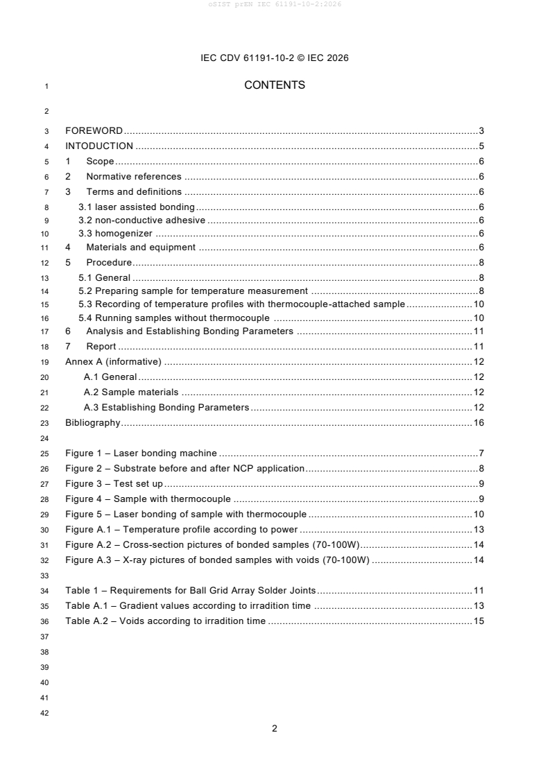
1 CONTENTS
3 FOREWORD . 3
4 INTODUCTION . 5
5 1 Scope . 6
6 2 Normative references . 6
7 3 Terms and definitions . 6
8 3.1 laser assisted bonding . 6
9 3.2 non-conductive adhesive . 6
10 3.3 homogenizer . 6
11 4 Materials and equipment . 6
12 5 Procedure . 8
13 5.1 General . 8
14 5.2 Preparing sample for temperature measurement . 8
15 5.3 Recording of temperature profiles with thermocouple-attached sample . 10
16 5.4 Running samples without thermocouple . 10
17 6 Analysis and Establishing Bonding Parameters . 11
18 7 Report . 11
19 Annex A (informative) . 12
20 A.1 General . 12
21 A.2 Sample materials . 12
22 A.3 Establishing Bonding Parameters . 12
23 Bibliography . 16
25 Figure 1 – Laser bonding machine . 7
26 Figure 2 – Substrate before and after NCP application . 8
27 Figure 3 – Test set up . 9
28 Figure 4 – Sample with thermocouple . 9
29 Figure 5 – Laser bonding of sample with thermocouple . 10
30 Figure A.1 – Temperature profile according to power . 13
31 Figure A.2 – Cross-section pictures of bonded samples (70-100W) . 14
32 Figure A.3 – X-ray pictures of bonded samples with voids (70-100W) . 14
34 Table 1 – Requirements for Ball Grid Array Solder Joints . 11
35 Table A.1 – Gradient values according to irradition time . 13
36 Table A.2 – Voids according to irradition time . 15
IEC CDV 61191-10-2 © IEC 2026
43 INTERNATIONAL ELECTROTECHNICAL COMMISSION
44 ____________
46 CIRCUIT BOARD ASSEMBLIES–
48 Part 10-2: Guideline for Establishing Bonding Parameters in Laser-
49 Assisted Bonding between Semiconductor Chip and Substrate
52 FOREWORD
53 1) The International Electrotechnical Commission (IEC) is a worldwide organization for standardization comprising
54 all national electrotechnical committees (IEC National Committees). The object of IEC is to promote international
55 co-operation on all questions concerning standardization in the electrical and electronic fields. To this end and
56 in addition to other activities, IEC publishes International Standards, Technical Specifications, Technical Reports,
57 Publicly Available Specifications (PAS) and Guides (hereafter referred to as "IEC Publication(s)"). Their
58 preparation is entrusted to technical committees; any IEC National Committee interested in the subject dealt with
59 may participate in this preparatory work. International, governmental and non-governmental organizations liaising
60 with the IEC also participate in this preparation. IEC collaborates closely with the International Organization for
61 Standardization (ISO) in accordance with conditions determined by agreement between the two organizations.
62 2) The formal decisions or agreements of IEC on technical matters express, as nearly as possible, an international
63 consensus of opinion on the relevant subjects since each technical committee has representation from all
64 interested IEC National Committees.
65 3) IEC Publications have the form of recommendations for international use and are accepted by IEC National
66 Committees in that sense. While all reasonable efforts are made to ensure that the technical content of IEC
67 Publications is accurate, IEC cannot be held responsible for the way in which they are used or for any
68 misinterpretation by any end user.
69 4) In order to promote international uniformity, IEC National Committees undertake to apply IEC Publications
70 transparently to the maximum extent possible in their national and regional publications. Any divergence between
71 any IEC Publication and the corresponding national or regional publication shall be clearly indicated in the latter.
72 5) IEC itself does not provide any attestation of conformity. Independent certification bodies provide conformity
73 assessment services and, in some areas, access to IEC marks of conformity. IEC is not responsible for any
74 services carried out by independent certification bodies.
75 6) All users should ensure that they have the latest edition of this publication.
76 7) No liability shall attach to IEC or its directors, employees, servants or agents including individual experts and
77 members of its technical committees and IEC National Committees for any personal injury, property damage or
78 other damage of any nature whatsoever, whether direct or indirect, or for costs (including legal fees) and
79 expenses arising out of the publication, use of, or reliance upon, this IEC Publication or any other IEC
80 Publications.
81 8) Attention is drawn to the Normative references cited in this publication. Use of the referenced publications is
82 indispensable for the correct application of this publication.
83 9) Attention is drawn to the possibility that some of the elements of this IEC Publication may be the subject of patent
84 rights. IEC shall not be held responsible for identifying any or all such patent rights
85 IEC 6XXXX has been prepared by subcommittee WG10 of IEC technical committee 91:
86 Electronics assembly technology. It is an International Standard.
87 The text of this standard is based on the following documents:
Draft Report on voting
91/XX/FDIS 91/XX/RVD
89 Full information on the voting for its approval can be found in the report on voting indicated in
90 the above table.
91 The language used for the development of this International Standard is English.
IEC CDV 61191-10-2 © IEC 2026
92 This document was drafted in accordance with ISO/IEC Directives, Part 2, and developed in
93 accordance with ISO/IEC Directives, Part 1 and ISO/IEC Directives, IEC Supplement available
94 at www.iec.ch/members_experts/refdocs. The main document types developed by IEC are
95 described in greater detail at www.iec.ch/publications.
96 The committee has decided that the contents of this document will remain unchanged until the
97 stability date indicated on the IEC website under webstore.iec.ch in the data related to the
98 specific document. At this date, the document will be
99 • reconfirmed,
100 • withdrawn,
101 • replaced by a revised edition, or
102 • amended.
105 The National Committees are requested to note that for this publication the stability date is 20
106 XX.
107 THIS TEXT IS INCLUDED FOR THE INFORMATION OF THE NATIONAL COMMITTEES AND
108 WILL BE DELETED AT THE PUBLICATION STAGE.
IEC CDV 61191-10-2 © IEC 2026
124 INTRODUCTION
125 In modern flip-chip packaging technology, the increasing number of input/output (I/O) terminals leads
126 to a reduction in pitch, which poses greater challenges with respect to package warpage issues.
127 Thermal compression bonding (TCB) has been used extensively in flip-chip interconnection
128 technology since conventional mass reflow techniques can induce reliability problems due to warpage
129 caused by coefficient of thermal expansion (CTE) mismatches between the semiconductor die and
130 substrate.
131 Although TCB is effective, its productivity is limited because it is a one-by-one process that takes
132 several seconds per bond. To enhance productivity while addressing warpage, a novel bonding
133 technology known as laser-assisted bonding (LAB) has been developed and implemented for
134 advanced flip-chip interconnections.
135 LAB utilizes laser irradiation to heat the component locally, allowing rapid solder reflow with minimal
136 substrate distortion. This approach enables improved throughput and reliability compared with
137 conventional thermal bonding methods.
IEC CDV 61191-10-2 © IEC 2026
140 CIRCUIT BOARD ASSEMBLIES–
142 Part 10-2: Guideline for Establishing Bonding Parameters in Laser-
143 Assisted Bonding between Semiconductor Chip and Subs
...