IEC TS 62607-6-5:2022
(Main)Nanomanufacturing - Key control characteristics - Part 6-5: Graphene-based materials - Contact and sheet resistance: transmission line measurement
Nanomanufacturing - Key control characteristics - Part 6-5: Graphene-based materials - Contact and sheet resistance: transmission line measurement
IEC TS 62607-6-5:2022(E) establishes a standardized method to determine the key control characteristics
contact resistance, and
sheet resistance for graphene-based materials and other two-dimensional materials by a
transmission line measurement. The method uses test structures applied to the 2D material by photolithographic methods consisting of several metal electrodes with increasing spacing between the electrodes. By a measurement of the voltage drop between different pairs of electrodes, sheet resistance and contact resistance can be calculated.
The method can be applied to any other two-dimensional materials which are subject to electrical metal contact on top of the materials.
The method provides accurate and reproducible results, if the electrical contact formed between the two-dimensional material and the metal electrodes provides ohmic contact property.
General Information
- Status
- Published
- Publication Date
- 13-Dec-2022
- Technical Committee
- TC 113 - Nanotechnology for electrotechnical products and systems
- Drafting Committee
- PT 62607-6-5 - TC 113/PT 62607-6-5
- Current Stage
- PPUB - Publication issued
- Start Date
- 14-Dec-2022
- Completion Date
- 13-Jan-2023
Overview
IEC TS 62607-6-5:2022 - Nanomanufacturing: Graphene-based materials - Contact resistance and sheet resistance: transmission line measurement (TLM) - defines a standardized, reproducible method to determine contact resistance and sheet resistance of graphene and other two-dimensional (2D) materials using the transmission line measurement. The technique uses photolithographically defined test structures with multiple metal electrodes at increasing spacings; voltage drops between electrode pairs are used to extract sheet and contact resistances. The method is applicable to any 2D material with metal contacts on top, provided the metal–material interface is ohmic.
Key topics and technical requirements
- Measurement principle: Transmission line measurement (TLM) patterns comprising sequential metal contacts with varied spacing; analysis of measured voltage/current to separate sheet resistance and contact resistance.
- Test structures: Photolithographic electrode patterns (rectangular channels, 2-point and 4-point probe TLM geometries) formed on the 2D material.
- Sample preparation: Recommended procedures for device fabrication and contact formation to ensure reliable, ohmic electrical contact.
- Measurement procedures: Recommended I–V testing workflows, suggested two‑point and four‑point probe implementations, and guidance on ensuring linear (ohmic) behavior.
- Limitations and constraints: Notes on non‑ohmic (Schottky) contacts and when TLM results may be invalid or require alternative interpretation.
- Reporting and case studies: Required result formats, example datasets for graphene and MoS2, and comparison of TLM with conventional four‑point probe approaches.
- Ancillary content: Recommended measurement equipment, apparatus, and simulations supporting reproducibility and interpretation.
Applications and users
Practical applications include:
- Quality control and process monitoring for graphene and 2D‑material manufacturing
- Electrical characterization during R&D of sensors, flexible electronics, interconnects, and optoelectronic devices
- Metrology and verification in academic and industrial research labs
- Supplier qualification and incoming inspection of 2D material films
Typical users:
- Materials scientists and device engineers
- Process engineers in fabs and pilot lines
- Metrology labs and standards bodies
- Test & validation teams for 2D-material-based products
Benefits
- Provides a standardized, repeatable protocol for separating contact and sheet resistances without requiring film thickness in calculations
- Promotes consistent reporting and comparability across labs and manufacturers
- Enhances traceability in nanomanufacturing workflows for 2D materials
Related standards
- Part of the IEC TS 62607 series (Nanomanufacturing - Key control characteristics). This document is intended to be compatible with other performance standards in the series and with broader IEC metrology guidance for electrical characterization of nanomaterials.
Keywords: IEC TS 62607-6-5:2022, transmission line measurement, TLM, graphene, sheet resistance, contact resistance, two-dimensional materials, nanomanufacturing, ohmic contact.
Get Certified
Connect with accredited certification bodies for this standard

BSMI (Bureau of Standards, Metrology and Inspection)
Taiwan's standards and inspection authority.
Sponsored listings
Frequently Asked Questions
IEC TS 62607-6-5:2022 is a technical specification published by the International Electrotechnical Commission (IEC). Its full title is "Nanomanufacturing - Key control characteristics - Part 6-5: Graphene-based materials - Contact and sheet resistance: transmission line measurement". This standard covers: IEC TS 62607-6-5:2022(E) establishes a standardized method to determine the key control characteristics contact resistance, and sheet resistance for graphene-based materials and other two-dimensional materials by a transmission line measurement. The method uses test structures applied to the 2D material by photolithographic methods consisting of several metal electrodes with increasing spacing between the electrodes. By a measurement of the voltage drop between different pairs of electrodes, sheet resistance and contact resistance can be calculated. The method can be applied to any other two-dimensional materials which are subject to electrical metal contact on top of the materials. The method provides accurate and reproducible results, if the electrical contact formed between the two-dimensional material and the metal electrodes provides ohmic contact property.
IEC TS 62607-6-5:2022(E) establishes a standardized method to determine the key control characteristics contact resistance, and sheet resistance for graphene-based materials and other two-dimensional materials by a transmission line measurement. The method uses test structures applied to the 2D material by photolithographic methods consisting of several metal electrodes with increasing spacing between the electrodes. By a measurement of the voltage drop between different pairs of electrodes, sheet resistance and contact resistance can be calculated. The method can be applied to any other two-dimensional materials which are subject to electrical metal contact on top of the materials. The method provides accurate and reproducible results, if the electrical contact formed between the two-dimensional material and the metal electrodes provides ohmic contact property.
IEC TS 62607-6-5:2022 is classified under the following ICS (International Classification for Standards) categories: 07.120 - Nanotechnologies; 17.140.20 - Noise emitted by machines and equipment; 97.040.50 - Small kitchen appliances. The ICS classification helps identify the subject area and facilitates finding related standards.
IEC TS 62607-6-5:2022 is available in PDF format for immediate download after purchase. The document can be added to your cart and obtained through the secure checkout process. Digital delivery ensures instant access to the complete standard document.
Standards Content (Sample)
IEC TS 62607-6-5 ®
Edition 1.0 2022-12
TECHNICAL
SPECIFICATION
colour
inside
Nanomanufacturing – Key control characteristics –
Part 6-5: Graphene-based materials – Contact resistance and sheet resistance:
transmission line measurement
All rights reserved. Unless otherwise specified, no part of this publication may be reproduced or utilized in any form
or by any means, electronic or mechanical, including photocopying and microfilm, without permission in writing from
either IEC or IEC's member National Committee in the country of the requester. If you have any questions about IEC
copyright or have an enquiry about obtaining additional rights to this publication, please contact the address below or
your local IEC member National Committee for further information.
IEC Secretariat Tel.: +41 22 919 02 11
3, rue de Varembé info@iec.ch
CH-1211 Geneva 20 www.iec.ch
Switzerland
About the IEC
The International Electrotechnical Commission (IEC) is the leading global organization that prepares and publishes
International Standards for all electrical, electronic and related technologies.
About IEC publications
The technical content of IEC publications is kept under constant review by the IEC. Please make sure that you have the
latest edition, a corrigendum or an amendment might have been published.
IEC publications search - webstore.iec.ch/advsearchform IEC Products & Services Portal - products.iec.ch
The advanced search enables to find IEC publications by a Discover our powerful search engine and read freely all the
variety of criteria (reference number, text, technical publications previews. With a subscription you will always have
committee, …). It also gives information on projects, replaced access to up to date content tailored to your needs.
and withdrawn publications.
Electropedia - www.electropedia.org
IEC Just Published - webstore.iec.ch/justpublished
The world's leading online dictionary on electrotechnology,
Stay up to date on all new IEC publications. Just Published
containing more than 22 300 terminological entries in English
details all new publications released. Available online and once
and French, with equivalent terms in 19 additional languages.
a month by email.
Also known as the International Electrotechnical Vocabulary
(IEV) online.
IEC Customer Service Centre - webstore.iec.ch/csc
If you wish to give us your feedback on this publication or need
further assistance, please contact the Customer Service
Centre: sales@iec.ch.
IEC TS 62607-6-5 ®
Edition 1.0 2022-12
TECHNICAL
SPECIFICATION
colour
inside
Nanomanufacturing – Key control characteristics –
Part 6-5: Graphene-based materials – Contact resistance and sheet resistance:
transmission line measurement
INTERNATIONAL
ELECTROTECHNICAL
COMMISSION
ICS 07.120 ISBN 978-2-8322-6224-5
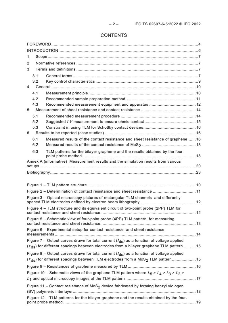
– 2 – IEC TS 62607-6-5:2022 © IEC 2022
CONTENTS
FOREWORD . 4
INTRODUCTION . 6
1 Scope . 7
2 Normative references . 7
3 Terms and definitions . 7
3.1 General terms . 7
3.2 Key control characteristics . 9
4 General . 10
4.1 Measurement principle . 10
4.2 Recommended sample preparation method. 11
4.3 Recommended measurement equipment and apparatus . 12
5 Measurement of sheet resistance and contact resistance . 14
5.1 Recommended measurement procedure . 14
5.2 Suggested I-V measurement to ensure ohmic contact . 15
5.3 Constraint in using TLM for Schottky contact devices . 16
6 Results to be reported (case studies) . 16
6.1 Measured results of the contact resistance and sheet resistance of graphene . 16
6.2 Measured results of the contact resistance of MoS . 18
6.3 TLM patterns for the bilayer graphene and the results obtained by the four-
point probe method . 18
Annex A (informative) Measurement results and the simulation results from various
setups . 20
Bibliography . 23
Figure 1 – TLM pattern structure . 10
Figure 2 – Determination of contact resistance and sheet resistance . 11
Figure 3 – Optical microscopy pictures of rectangular TLM channels and differently
spaced TLM electrodes defined by electron beam lithography . 12
Figure 4 – TLM structure and its equivalent circuit of two-point probe (2PP) TLM for
contact resistance and sheet resistance. 12
Figure 5 – Schematic view of four-point probe (4PP) TLM pattern for measuring
contact resistance and sheet resistance. 13
Figure 6 – Experimental setup for contact resistance and sheet resistance
measurements . 14
Figure 7 – Output curves drawn for total current (I ) as a function of voltage applied
ds
(V ) for different spacings between electrodes from a bilayer graphene TLM pattern . 15
ds
Figure 8 – Output curves drawn for total current (I ) as a function of voltage applied
ds
(V ) for different spacings between TLM electrodes from a MoS TLM pattern . 15
ds 2
Figure 9 – Resistances of graphene measured by TLM . 16
Figure 10 – Schematic views of the graphene TLM pattern where L > L > L > L >
5 4 3 2
L and optical microscopy images of the TLM pattern . 17
Figure 11 – Contact resistance of MoS device fabricated by forming benzyl viologen
(BV) polymeric interlayer. 18
Figure 12 – TLM patterns for the bilayer graphene and the results obtained by the four-
point probe method . 19
Figure A.1 – Comparison of TLM two-point probe and four-point probe setups . 21
Table 1 – Contact resistance and sheet resistance of graphene, obtained from
different plasma etching conditions . 17
Table A.1 – Contact resistance measurement by TLM and conventional four-point
probe methods based upon the case study of Figure 12 . 20
Table A.2 – Sheet resistance measurement by TLM and conventional four-point probe
methods based upon the case study of Figure 12 . 21
Table A.3 – Simulation of contact resistance and sheet resistance results from TLM
two-point probe and four-point probe methods . 22
– 4 – IEC TS 62607-6-5:2022 © IEC 2022
INTERNATIONAL ELECTROTECHNICAL COMMISSION
____________
NANOMANUFACTURING – KEY CONTROL CHARACTERISTICS –
Part 6-5: Graphene-based materials – Contact resistance and sheet
resistance: transmission line measurement
FOREWORD
1) The International Electrotechnical Commission (IEC) is a worldwide organization for standardization comprising
all national electrotechnical committees (IEC National Committees). The object of IEC is to promote
international co-operation on all questions concerning standardization in the electrical and electronic fields. To
this end and in addition to other activities, IEC publishes International Standards, Technical Specifications,
Technical Reports, Publicly Available Specifications (PAS) and Guides (hereafter referred to as “IEC
Publication(s)”). Their preparation is entrusted to technical committees; any IEC National Committee interested
in the subject dealt with may participate in this preparatory work. International, governmental and non-
governmental organizations liaising with the IEC also participate in this preparation. IEC collaborates closely
with the International Organization for Standardization (ISO) in accordance with conditions determined by
agreement between the two organizations.
2) The formal decisions or agreements of IEC on technical matters express, as nearly as possible, an international
consensus of opinion on the relevant subjects since each technical committee has representation from all
interested IEC National Committees.
3) IEC Publications have the form of recommendations for international use and are accepted by IEC National
Committees in that sense. While all reasonable efforts are made to ensure that the technical content of IEC
Publications is accurate, IEC cannot be held responsible for the way in which they are used or for any
misinterpretation by any end user.
4) In order to promote international uniformity, IEC National Committees undertake to apply IEC Publications
transparently to the maximum extent possible in their national and regional publications. Any divergence
between any IEC Publication and the corresponding national or regional publication shall be clearly indicated in
the latter.
5) IEC itself does not provide any attestation of conformity. Independent certification bodies provide conformity
assessment services and, in some areas, access to IEC marks of conformity. IEC is not responsible for any
services carried out by independent certification bodies.
6) All users should ensure that they have the latest edition of this publication.
7) No liability shall attach to IEC or its directors, employees, servants or agents including individual experts and
members of its technical committees and IEC National Committees for any personal injury, property damage or
other damage of any nature whatsoever, whether direct or indirect, or for costs (including legal fees) and
expenses arising out of the publication, use of, or reliance upon, this IEC Publication or any other IEC
Publications.
8) Attention is drawn to the Normative references cited in this publication. Use of the referenced publications is
indispensable for the correct application of this publication.
9) Attention is drawn to the possibility that some of the elements of this IEC Publication may be the subject of
patent rights. IEC shall not be held responsible for identifying any or all such patent rights.
IEC TS 62607-6-5 has been prepared by IEC technical committee 113: Nanotechnology for
electrotechnical products and systems. It is a Technical Specification.
The text of this Technical Specification is based on the following documents:
Draft Report on voting
113/677/DTS 113/709/RVDTS
Full information on the voting for its approval can be found in the report on voting indicated in
the above table.
The language used for the development of this Technical Specification is English.
This document was drafted in accordance with ISO/IEC Directives, Part 2, and developed in
accordance with ISO/IEC Directives, Part 1 and ISO/IEC Directives, IEC Supplement,
available at www.iec.ch/members_experts/refdocs. The main document types developed by
IEC are described in greater detail at www.iec.ch/publications.
A list of all parts in the IEC TS 62607 series, published under the general title
Nanomanufacturing – Key control characteristics, can be found on the IEC website.
The committee has decided that the contents of this document will remain unchanged until the
stability date indicated on the IEC website under webstore.iec.ch in the data related to the
specific document. At this date, the document will be
• reconfirmed,
• withdrawn,
• replaced by a revised edition, or
• amended.
IMPORTANT – The "colour inside" logo on the cover page of this document indicates that it
contains colours which are considered to be useful for the correct understanding of its
contents. Users should therefore print this document using a colour printer.
– 6 – IEC TS 62607-6-5:2022 © IEC 2022
INTRODUCTION
Technical Specifications for contact resistance and sheet resistance of two-dimensional
materials provide a proper definition of contact resistance and sheet resistance measurement
and an electrical characterization of two-dimensional materials. This document includes
recommended conditions for a sample preparation and recommended method to measure
contact resistance and sheet resistance of two-dimensional materials under test in the
referenced background research results. Here, the transmission line measurement (TLM) is
used which had been used to measure both contact resistance and sheet resistance for
conventional bulk semiconductor devices including silicon devices. TLM devices are formed
with various spacings between contacts from which contact resistance and sheet resistance
are determined from voltage measured. Thickness of the atomic thin 2D materials cannot be
defined clearly when the layers are ultrathin near monolayer, and therefore it is difficult to
express the thickness-dependent electronic resistivities of the devices fabricated by using 2D
materials. TLM is used conveniently to determine contact resistance and sheet resistance of
2D materials since it does not require thickness of tested materials to be included in the
calculation procedure.
The objectives of this document are to
a) define the contact resistance and sheet resistance of two-dimensional materials;
b) specify the methodology for contact resistance and sheet resistance measurements of
two-dimensional materials using transmission line measurement (TLM);
c) provide a contact formation method for two-dimensional materials with ohmic contact
property which is an essential prerequisite;
d) establish units for the quantitative characteristics of contact resistance and sheet
resistance for two-dimensional materials;
e) provide relevant case studies;
f) provide relevant references.
This document is meant to be a general document that can be applied to two-dimensional
materials and their applications. It is the intent of this document to be compatible with and
work in conjunction with the performance standards defined in the IEC TS 62607 series.
NANOMANUFACTURING – KEY CONTROL CHARACTERISTICS –
Part 6-5: Graphene-based materials – Contact resistance and sheet
resistance: transmission line measurement
1 Scope
This part of IEC TS 62607 establishes a standardized method to determine the key control
characteristics
• contact resistance, and
• sheet resistance
for graphene-based materials and other two-dimensional materials by a
• transmission line measurement.
The method uses test structures applied to the 2D material by photolithographic methods
consisting of several metal electrodes with increasing spacing between the electrodes. By a
measurement of the voltage drop between different pairs of electrodes, sheet resistance and
contact resistance can be calculated.
• The method can be applied to any other two-dimensional materials which are subject to
electrical metal contact on top of the materials.
• The method provides accurate and reproducible results, if the electrical contact formed
between the two-dimensional material and the metal electrodes provides ohmic contact
property.
2 Normative references
There are no normative references in this document.
3 Terms and definitions
For the purposes of this document, the following terms and definitions apply.
ISO and IEC maintain terminological databases for use in standardization at the following
addresses:
• IEC Electropedia: available at http://www.electropedia.org/
• ISO Online browsing platform: available at http://www.iso.org/obp
3.1 General terms
3.1.1
detail specification
DS
specification based on a blank detail specification with assigned values and attributes
Note 1 to entry: The properties listed in the detail specification are usually a subset of the key control
characteristics listed in the relevant blank detail specification. The industrial partners define only those properties
which are required for the intended application.
Note 2 to entry: Detail specifications are defined by the industrial partners. Standards development organizations
will be involved only if there is a general need for a detail specification in an industrial sector.
– 8 – IEC TS 62607-6-5:2022 © IEC 2022
Note 3 to entry: The industrial partners can define additional key control characteristics if they are not listed in the
blank detail specification.
3.1.2
graphene
graphene layer
single-layer graphene
monolayer graphene
single layer of carbon atoms with each atom bound to three neighbours in a honeycomb
structure
Note 1 to entry: It is an important building block of many carbon nano-objects.
Note 2 to entry: As graphene is a single layer, it is also sometimes called monolayer graphene or single-layer
graphene and abbreviated as 1LG to distinguish it from bilayer graphene (2LG) and few-layer graphene (FLG).
Note 3 to entry: Graphene has edges and can have defects and grain boundaries where the bonding is disrupted.
[SOURCE: ISO/TS 80004-13:2017, 3.1.2.1]
3.1.3
bilayer graphene
2LG
two-dimensional material consisting of two well-defined stacked graphene layers
Note 1 to entry: If the stacking registry is known, it can be specified separately, for example, as "Bernal stacked
bilayer graphene".
[SOURCE: ISO/TS 80004-13:2017, 3.1.2.6]
3.1.4
few-layer graphene
FLG
two-dimensional material consisting of three to ten well-defined stacked graphene layers
[SOURCE: ISO/TS 80004-13:2017, 3.1.2.10]
3.1.5
two-dimensional material
2D material
material, consisting of one or several layers with the atoms in each layer strongly bonded to
neighbouring atoms in the same layer, which has one dimension, its thickness, in the
nanoscale or smaller and the other two dimensions generally at larger scales.
Note 1 to entry: The number of layers when a two-dimensional material becomes a bulk material varies depending
on both the material being measured and its properties. In the case of graphene layers, it is a two-dimensional
material up to 10 layers thick for electrical measurements, beyond which the electrical properties of the material
are not distinct from those for the bulk (also known as graphite).
Note 2 to entry: Interlayer bonding is distinct from and weaker than intralayer bonding.
Note 3 to entry: Each layer can contain more than one element.
Note 4 to entry: A two-dimensional material can be a nanoplate.
[SOURCE: ISO/TS 80004-13:2017, 3.1.1.1]
3.2 Key control characteristics
3.2.1
key control characteristic
KCC
material property or intermediate product characteristic which can affect safety or compliance
with regulations, fit, function, performance, quality, reliability or subsequent processing of the
final product
Note 1 to entry: The measurement of a key control characteristic is described in a standardized measurement
procedure with known accuracy and precision.
Note 2 to entry: It is possible to define more than one measurement method for a key control characteristic if the
correlation of the results is well-defined and known.
3.2.2
sheet resistance
measure of the resistance of a thin film that is nominally uniform in thickness
Note 1 to entry: Sheet resistance can be measured together with contact resistance by TLM for 2D materials, as
shown in Figure 2.
Note 2 to entry: Sheet resistance is one of a material’s properties. The SI unit of measure of sheet resistance is
the ohm per square (Ω/sq.).
3.2.3
contact resistance
measure of the contribution of the contacting interfaces to the total resistance of thin films
that are nominally uniform in thickness
Note 1 to entry: Contact resistance can be measured together with sheet resistance by TLM for 2D materials, as
shown in Figure 2.
Note 2 to entry: Contact resistance is a property that exists between a metal and a semiconducting (or
conducting) material. Contacts need to supply necessary electrical current.
[SOURCE: Schroder [1], Pages 127, 131]
3.3 Terms related to the measurement method
3.3.1
transfer length
L
T
measuring distance over which most of the current flows from a semiconductor (or conducting
material) into a metal or from a metal into a semiconductor (or conducting material)
[SOURCE: Schroder [1], Page 140]
3.3.2
transmission line measurement
TLM
measuring method to determine sheet resistance of a layer and contact resistance between a
layer and an applied electrode by the formation of a set of electrodes and a measurement of
the voltage drop between the electrodes
Note 1 to entry: In some cases, TLM is used as abbreviation for transfer length measurement, but this represents
the same technique as the transmission line measurement.
[SOURCE: Schroder [1], Pages 1
...


Questions, Comments and Discussion
Ask us and Technical Secretary will try to provide an answer. You can facilitate discussion about the standard in here.
Loading comments...