SIST EN 60191-6-3:2002
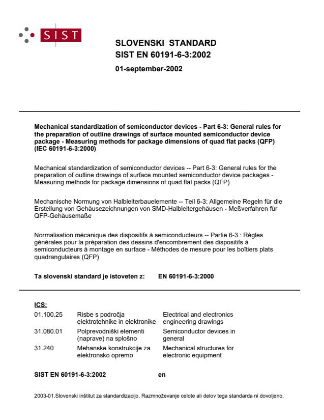
(Main)Mechanical standardization of semiconductor devices -- Part 6-3: General rules for the preparation of outline drawings of surface mounted semiconductor device packages - Measuring methods for package dimensions of quad flat packs (QFP)
Mechanical standardization of semiconductor devices -- Part 6-3: General rules for the preparation of outline drawings of surface mounted semiconductor device packages - Measuring methods for package dimensions of quad flat packs (QFP)
Stipulates a method for quad flat packs measuring dimensions which are classified into Form E.
Mechanische Normung von Halbleiterbauelemente -- Teil 6-3: Allgemeine Regeln für die Erstellung von Gehäusezeichnungen von SMD-Halbleitergehäusen - Meßverfahren für QFP-Gehäusemaße
Normalisation mécanique des dispositifs à semiconducteurs -- Partie 6-3 : Règles générales pour la préparation des dessins d'encombrement des dispositifs à semiconducteurs à montage en surface - Méthodes de mesure pour les boîtiers plats quadrangulaires (QFP)
La CEI 60191-6-3:2000 stipule une méthode de mesure des dimensions des boîtiers plats quadrangulaires (QFP) qui sont classés dans la forme E.
Mechanical standardization of semiconductor devices - Part 6-3: General rules for the preparation of outline drawings of surface mounted semiconductor device package - Measuring methods for package dimensions of quad flat packs (QFP) (IEC 60191-6-3:2000)
General Information
- Status
- Published
- Publication Date
- 31-Aug-2002
- Current Stage
- 6060 - National Implementation/Publication (Adopted Project)
- Start Date
- 01-Sep-2002
- Due Date
- 01-Sep-2002
- Completion Date
- 01-Sep-2002
Overview
EN 60191-6-3:2000 (identical to IEC 60191-6-3:2000) specifies measuring methods for package dimensions of quad flat packs (QFP) classified as Form E. It is a part of the mechanical standardization series for surface-mounted semiconductor device packages and defines how outline drawing dimensions are to be measured and guaranteed to users.
Key topics and technical requirements
- Scope and form: Applies specifically to QFP package dimensions classified as Form E and supplements the general rules in IEC 60191-6.
- Measurement principle: Dimensions are normally measured with the package mounted on a printed circuit board or a seating plane (surface plate); measurements may be done manually or automatically.
- Datum definition: Establishes package datum axes (A and B) from centres of opposite sides and prescribes how to correct angular deviations so axes are rectangular.
- Primary dimensions covered:
- Overall width (HE) and overall length (HD)
- Package width (D) and package length (E)
- Mounting height (A) (height from seating plane to highest point including warpage)
- Stand-off (A1) (lowest point above seating plane)
- Body thickness (A2) (thickness of package body)
- Lead dimensions: lead widths (b, b1), lead thicknesses (c, c1), and soldered portion length (Lp)
- Positional tolerance of terminal tips (method to compute deviations from theoretical centres)
- Coplanarity (y) (vertical spread of lowest lead surfaces referenced to a virtual plane)
- Measuring methods and remarks:
- Procedures describe placement on surface plate, reference alignment, and how to measure specific features (side, top or between parallel plates for body thickness).
- When measurement destroys the package, dimensions may be calculated from other values or replaced by representative values.
- Annexes and normative references (notably IEC 60191-6:1990) are incorporated by reference.
Applications and who uses this standard
- Semiconductor package designers and mechanical engineers creating outline drawings for QFPs.
- IC manufacturers and test/quality engineers for acceptance, incoming inspection and process control.
- PCB designers and contract manufacturers ensuring component fit, solderability and clearance.
- Inspection equipment and metrology suppliers implementing automated optical or contact measurement procedures.
- Standards bodies and technical documentation teams requiring consistent dimensional definitions.
Related standards
- IEC 60191-6:1990 - General rules for the preparation of outline drawings of surface mounted semiconductor device packages (normative reference).
- EN/IEC 60191 series - other parts cover mechanical standardization of semiconductor devices.
Keywords: EN 60191-6-3:2000, IEC 60191-6-3, QFP measuring methods, quad flat pack, package dimensions, Form E, coplanarity, lead thickness, mounting height, datum, outline drawings.
Frequently Asked Questions
SIST EN 60191-6-3:2002 is a standard published by the Slovenian Institute for Standardization (SIST). Its full title is "Mechanical standardization of semiconductor devices -- Part 6-3: General rules for the preparation of outline drawings of surface mounted semiconductor device packages - Measuring methods for package dimensions of quad flat packs (QFP)". This standard covers: Stipulates a method for quad flat packs measuring dimensions which are classified into Form E.
Stipulates a method for quad flat packs measuring dimensions which are classified into Form E.
SIST EN 60191-6-3:2002 is classified under the following ICS (International Classification for Standards) categories: 01.100.25 - Electrical and electronics engineering drawings; 31.080.01 - Semiconductor devices in general; 31.240 - Mechanical structures for electronic equipment. The ICS classification helps identify the subject area and facilitates finding related standards.
SIST EN 60191-6-3:2002 is available in PDF format for immediate download after purchase. The document can be added to your cart and obtained through the secure checkout process. Digital delivery ensures instant access to the complete standard document.
Standards Content (Sample)
2003-01.Slovenski inštitut za standardizacijo. Razmnoževanje celote ali delov tega standarda ni dovoljeno.Mechanical standardization of semiconductor devices - Part 6-3: General rules for the preparation of outline drawings of surface mounted semiconductor device package - Measuring methods for package dimensions of quad flat packs (QFP) (IEC 60191-6-3:2000)Mechanische Normung von Halbleiterbauelemente -- Teil 6-3: Allgemeine Regeln für die Erstellung von Gehäusezeichnungen von SMD-Halbleitergehäusen - Meßverfahren für QFP-GehäusemaßeNormalisation mécanique des dispositifs à semiconducteurs -- Partie 6-3 : Règles générales pour la préparation des dessins d'encombrement des dispositifs à semiconducteurs à montage en surface - Méthodes de mesure pour les boîtiers plats quadrangulaires (QFP)Mechanical standardization of semiconductor devices -- Part 6-3: General rules for the preparation of outline drawings of surface mounted semiconductor device packages - Measuring methods for package dimensions of quad flat packs (QFP)31.240Mehanske konstrukcije za elektronsko opremoMechanical structures for electronic equipment31.080.01Polprevodniški elementi (naprave) na splošnoSemiconductor devices in general01.100.25Electrical and electronics engineering drawingsICS:Ta slovenski standard je istoveten z:EN 60191-6-3:2000SIST EN 60191-6-3:2002en01-september-2002SIST EN 60191-6-3:2002SLOVENSKI
STANDARD
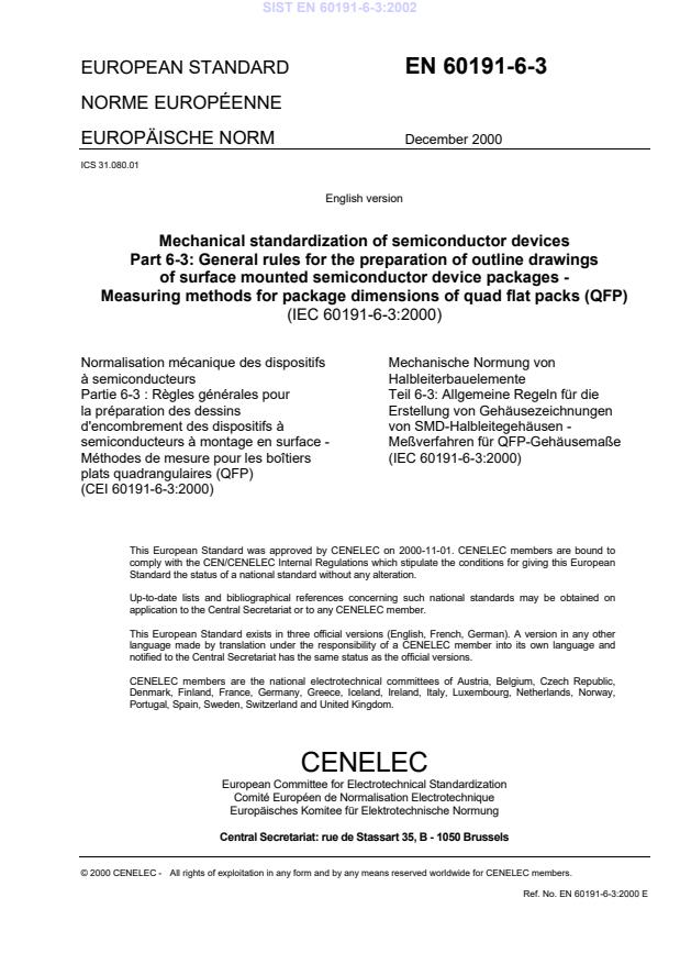
EUROPEAN STANDARD
EN 60191-6-3 NORME EUROPÉENNE EUROPÄISCHE NORM
December 2000 CENELEC European Committee for Electrotechnical Standardization Comité Européen de Normalisation Electrotechnique Europäisches Komitee für Elektrotechnische Normung
Central Secretariat: rue de Stassart 35, B - 1050 Brussels
© 2000 CENELEC - All rights of exploitation in any form and by any means reserved worldwide for CENELEC members.
Ref. No. EN 60191-6-3:2000 E
ICS 31.080.01
English version
Mechanical standardization of semiconductor devices Part 6-3: General rules for the preparation of outline drawings
of surface mounted semiconductor device packages -
Measuring methods for package dimensions of quad flat packs (QFP) (IEC 60191-6-3:2000)
Normalisation mécanique des dispositifs à semiconducteurs Partie 6-3 : Règles générales pour la préparation des dessins d'encombrement des dispositifs à semiconducteurs à montage en surface - Méthodes de mesure pour les boîtiers plats quadrangulaires (QFP) (CEI 60191-6-3:2000)
Mechanische Normung von Halbleiterbauelemente Teil 6-3: Allgemeine Regeln für die Erstellung von Gehäusezeichnungen von SMD-Halbleitegehäusen -
Meßverfahren für QFP-Gehäusemaße (IEC 60191-6-3:2000)
This European Standard was approved by CENELEC on 2000-11-01. CENELEC members are bound to comply with the CEN/CENELEC Internal Regulations which stipulate the conditions for giving this European Standard the status of a national standard without any alteration.
Up-to-date lists and bibliographical references concerning such national standards may be obtained on application to the Central Secretariat or to any CENELEC member.
This European Standard exists in three official versions (English, French, German). A version in any other language made by translation under the responsibility of a CENELEC member into its own language and notified to the Central Secretariat has the same status as the official versions.
CENELEC members are the national electrotechnical committees of Austria, Belgium, Czech Republic, Denmark, Finland, France, Germany, Greece, Iceland, Ireland, Italy, Luxembourg, Netherlands, Norway, Portugal, Spain, Sweden, Switzerland and United Kingdom.
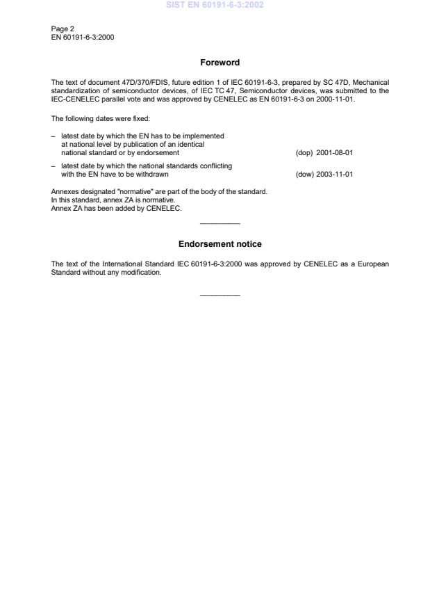
Page 2 EN 60191-6-3:2000 Foreword The text of document 47D/370/FDIS, future edition 1 of IEC 60191-6-3, prepared by SC 47D, Mechanical standardization of semiconductor devices, of IEC TC 47, Semiconductor devices, was submitted to the IEC-CENELEC parallel vote and was approved by CENELEC as EN 60191-6-3 on 2000-11-01. The following dates were fixed: – latest date by which the EN has to be implemented
at national level by publication of an identical
national standard or by endorsement
(dop) 2001-08-01 – latest date by which the national standards conflicting
with the EN have to be withdrawn
(dow) 2003-11-01 Annexes designated "normative" are part of the body of the standard.
In this standard, annex ZA is normative. Annex ZA has been added by CENELEC. __________ Endorsement notice The text of the International Standard IEC 60191-6-3:2000 was approved by CENELEC as a European Standard without any modification. __________ SIST EN 60191-6-3:2002
Page 3 EN 60191-6-3:2000
Annex ZA
(normative)
Normative references to international publications
with their corresponding European publications This European Standard incorporates by dated or undated reference, provisions from other publications. These normative references are cited at the appropriate places in the text and the publications are listed hereafter. For dated references, subsequent amendments to or revisions of any of these publications apply to this European Standard only when incorporated in it by amendment or revision. For undated references the latest edition of the publication referred to applies (including amendments). NOTE When an international publication has been modified by common modifications, indicated by (mod), the relevant EN/HD applies. Publication Year Title
EN/HD Year IEC 60191-6 1990 Mechanical standardization of semiconductor devices Part 6: General rules for the preparation of outline drawings of surface mounted semiconductor device packages
- -
INTERNATIONALSTANDARDIEC60191-6-3First edition2000-09Mechanical standardization ofsemiconductor devices –Part 6-3:General rules for the preparation ofoutline drawings of surface mountedsemiconductor device packages –Measuring methods for package dimensionsof quad flat packs (QFP)Normalisation mécanique des dispositifs à semiconducteurs –Partie 6-3:Règles générales pour la préparation des dessinsd’encombrement des dispositifs à semiconducteursà montage en surface – Méthodes de mesure pourles boîtiers plats quadrangulaires (QFP)PRICE CODE IEC 2000
Copyright - all rights reservedNo part of this publication may be reproduced or utilized in any form or by any means, electronic ormechanical, including photocopying and microfilm, without permission in writing from the publisher.International Electrotechnical Commission3, rue de Varembé
Geneva, SwitzerlandTelefax: +41 22 919 0300e-mail: inmail@iec.ch IEC web site
http://www.iec.chQFor price, see current catalogue Commission Electrotechnique Internationale International Electrotechnical CommissionSIST EN 60191-6-3:2002
– 2 –60191-6-3 IEC:2000(E)INTERNATIONAL ELECTROTECHNICAL COMMISSION____________MECHANICAL STANDARDIZATION OF SEMICONDUCTOR DEVICES –Part 6-3: General rules for the preparation of outline drawingsof surface mounted semiconductor device packages –Measuring methods for package dimensions of quad flat packs (QFP)FOREWORD1)The IEC (International Electrotechnical Commission) is a worldwide organization for standardization comprisingall national electrotechnical committees (IEC National Committees). The object of the IEC is to promoteinternational co-operation on all questions concerning standardization in the electrical and electronic fields. Tothis end and in addition to other activities, the IEC publishes International Standards. Their preparation isentrusted to technical committees; any IEC National Committee interested in the subject dealt with mayparticipate in this preparatory work. International, governmental and non-governmental organizations liaisingwith the IEC also participate in this preparation. The IEC collaborates closely with the InternationalOrganization for Standardization (ISO) in accordance with conditions determined by agreement between thetwo organizations.2)The formal decisions or agreements of the IEC on technical matters express, as nearly as possible, aninternational consensus of opinion on the relevant subjects since each technical committee has representationfrom all interested National Committees.3)The documents produced have the form of recommendations for international use and are published in the formof standards, technical specifications, technical reports or guides and they are accepted by the NationalCommittees in that sense.4)
In order to promote international unification, IEC National Committees undertake to apply IEC InternationalStandards transparently to the maximum extent possible in their national and regional standards. Anydivergence between the IEC Standard and the corresponding national or regional standard shall be clearlyindicated in the latter.5)
The IEC provides no marking procedure to indicate its approval and cannot be rendered responsible for anyequipment declared to be in conformity with one of its standards.6)
Attention is drawn to the possibility that some of the elements of this International Standard may be the subjectof patent rights. The IEC shall not be held responsible for identifying any or all such patent rights.International Standard IEC 60191-6-3 has been prepared by subcommittee 47D: Mechanicalstandardization of semiconductor devices, of IEC technical committee 47: Semiconductordevices.The text of this standard is based on the following documents:FDISReport on voting47D/370/FDIS47D/388/RVDFull information on the voting for the approval of this standard can be found in the report onvoting indicated in the above table.This publication has been drafted in accordance with the ISO/IEC Directives, Part 3.SIST EN 60191-6-3:2002
60191-6-3 IEC:2000(E)– 3 –The committee has decided that the contents of this publication will remain unchanged until 2003.At this date, the publication will bereconfirmed;withdrawn;replaced by a revised edition, oramended.A bilingual version of this publication may be issued at a later date.SIST EN 60191-6-3:2002
– 4 –60191-6-3 IEC:2000(E)MECHANICAL STANDARDIZATION OF SEMICONDUCTOR DEVICES –Part 6-3: General rules for the preparation of outline drawingsof surface mounted semiconductor device packages –Measuring methods for package dimensions of quad flat packs (QFP)1 ScopeThis part of IEC 60191 stipulates a method for quad flat packs (QFP) measuring dimensionswhich are classified into Form E.2 Normative referencesThe following normative documents contain provisions which, through reference in this t
...


Questions, Comments and Discussion
Ask us and Technical Secretary will try to provide an answer. You can facilitate discussion about the standard in here.
Loading comments...