

oSIST prEN IEC 63470:2026
(Main)Guideline for gate oxide reliability and robustness evaluation procedures for silicon carbide power mosfets (Fast Track)
- Status
- Not Published
- Public Enquiry End Date
- 30-Sep-2026
- Technical Committee
- I11 - Imaginarni 11
- Current Stage
- 4020 - Public enquire (PE) (Adopted Project)
- Start Date
- 23-Jul-2026
- Due Date
- 10-Dec-2026
- Completion Date
- 29-Sep-2026

oSIST prEN IEC 63470:2026 is the Slovenian identical adoption of prEN IEC 63470:2026, an IEC fast-track guideline on gate oxide reliability and robustness evaluation for silicon carbide power MOSFETs. It specifies test procedures for time-dependent dielectric breakdown, ramped breakdown, and related defect checks so engineers can compare intrinsic lifetime and extrinsic failure behavior in SiC MOS devices.
What does oSIST prEN IEC 63470:2026 specify?
oSIST prEN IEC 63470:2026 specifies practical guidance for evaluating gate oxide reliability in SiC power MOS devices. It focuses on MOS devices on silicon carbide substrates, especially thick gate oxides where hard breakdown is expected and lifetime can be studied with stress testing.
The guideline is organized into six clauses and three informative annexes.
| Annex | What it covers |
|---|---|
| Annex A | Current based methods for lifetime and breakdown evaluation |
| Annex B | Supplemental data analysis, including failure distributions, area scaling, lifetime extrapolation, Fowler-Nordheim tunneling, and ramped gate lifetime extraction |
| Annex C | Bibliography |
Clause 1 states the scope, Clause 2 lists normative references, Clause 3 gives terms, definitions and letter symbols, Clause 4 covers intrinsic gate oxide quality by constant-voltage breakdown stress, Clause 5 covers inline monitoring by ramped breakdown testing, and Clause 6 covers accompanying tests for gate oxide defects and extrinsic gate oxide quality.
In practice, the document is about choosing a stress method, collecting failure data, and interpreting the results for product qualification, process monitoring, and failure analysis. It also keeps the focus on practical device testing rather than on setting lifetime limits or use conditions.
What are the key requirements of oSIST prEN IEC 63470:2026?
oSIST prEN IEC 63470:2026 recommends several test approaches, with the main choice depending on whether the goal is lifetime extraction, process monitoring, or extrinsic defect screening. The most important point is to match the test to the question being asked.
Use representative devices and consistent stress conditions
Clause 4 recommends testing comparable groups of devices from standard production, with known good parts and consistent failure criteria. For lifetime work, the guideline prefers the actual product device where possible, with gate polarity matching the real use case.
This matters because capacitors can behave more simply than transistors, and a less representative structure can give overly optimistic results. The guideline also recommends enough samples per stress condition, typically at least 25 devices, so the failure distribution is meaningful.
Separate high-field and low-field behavior
Clause 4 distinguishes high electric field stress from low electric field stress. High-field tests are useful for comparing process variations and separating intrinsic and extrinsic failures, but the observed parameters are not meant for lifetime extrapolation.
Low-field tests are the ones intended for lifetime projection toward use conditions. The guideline recommends multiple stress levels and temperatures, Weibull analysis, and the linear E-model as the conservative default for extrapolation.
Use Weibull statistics for lifetime and quality metrics
Clause 4.3.1 and 4.3.2 recommend Weibull slope and representative failure times such as t63 or t50 as the main quality metrics. For product quality testing, the guideline advises stressing at several gate voltages above the use voltage until about 63% of the population fails, then projecting lifetime back to the use condition.
This matters in practice because the same Weibull slope should describe the intrinsic dielectric behavior across stress conditions, while outliers can indicate extrinsic defects. The document also notes that the chosen stress levels should be high enough to produce failures in a practical time window, but not so high that they trigger the wrong failure mechanism.
Monitor ramped breakdown for fast process control
Clause 5 recommends ramped voltage stress or ramped current stress for quick inline monitoring of oxide quality. The ramp should be fine enough to resolve breakdown voltage clearly, and the ramp rate should be slow enough to avoid changing the failure mechanism.
The practical value is speed: a large number of samples can be screened quickly on a wafer probe station with a heated chuck. The guideline also recommends keeping the full I-V data so the breakdown event and Fowler-Nordheim behavior can be checked.
Use step-stress and marathon testing for extrinsic defects
Clause 6.1 describes a step-wise increased gate voltage test with gate-source leakage checks before and after each stress step. Clause 6.2 describes a Marathon Test with a large sample count and long stress time near burn-in-like conditions, but below intrinsic wear-out.
These methods help separate intrinsic oxide wear-out from early-life failures caused by extrinsic defects. In practice, they are used to estimate post-screening field-failure probability and to judge whether early failures would matter within the intended product lifetime.
Consider current-based methods when they fit the question
Annex A presents constant-current stress as an alternative way to assess dielectric lifetime, using charge to breakdown and current density rather than gate voltage. The annex notes that this is especially useful when the current characteristic itself carries useful lifetime information.
That matters when the goal is to compare dielectric behavior from a current perspective or to cross-check voltage-based results. The annex also stresses that the stress current density must be low enough to keep the failure mechanism aligned with application conditions.
What terms does oSIST prEN IEC 63470:2026 define?
oSIST prEN IEC 63470:2026 defines the key terms used in gate oxide stress testing and lifetime analysis.
- TDDB - Time-dependent dielectric breakdown; breakdown testing where time is the main stress variable.
- CVS - Constant voltage stress; the usual TDDB condition with fixed gate voltage during stress.
- CCS - Constant current stress; a TDDB condition where current density is held constant.
- RBD - Ramped breakdown; a breakdown test using ramped voltage stress or ramped current stress.
- tBD - Time to breakdown; the failure time used in lifetime analysis, often linked to Weibull statistics.
- tox - Oxide thickness; the gate dielectric thickness used in field calculations and lifetime interpretation.
- Eox - Oxide field; the electric field across the gate oxide, derived from voltage and thickness.
- Q - Charge to breakdown; the charge accumulated up to failure in a constant current stress test.
Who uses oSIST prEN IEC 63470:2026?
oSIST prEN IEC 63470:2026 is used by engineers and organizations that design, qualify, test, or buy SiC power semiconductor devices. Typical users include reliability engineers, process engineers, device designers, test labs, quality managers, and buyers working with MOSFETs, MOS capacitors, and IGBTs.
It is especially relevant when a team needs to compare process changes, qualify a new dielectric or wafer flow, screen early failures, or estimate oxide lifetime under use conditions. The introduction also shows that the document was developed by industry experts in power semiconductors, power supplies, and test equipment.
Which standards are used with oSIST prEN IEC 63470:2026?
oSIST prEN IEC 63470:2026 is based on JEDEC JEP194 and also cites the following normative references.
- JEP001A - Foundry Process Qualification Guidelines, used for process qualification context.
- JEP122H - Failure Mechanisms and Models for Silicon Semiconductor Devices, used for failure-mechanism and modeling background.
- JESD35-A - Procedure for the Wafer-Level Testing of Thin Dielectrics, used for wafer-level thin-dielectric test practice.
- JESD35-2 - Test Criteria for the Wafer-Level Testing of Thin Dielectrics, used for criteria tied to wafer-level testing.
- JESD47J.01 - Stress-Test-Driven Qualification of Integrated Circuits, used for qualification and stress-test framing.
- JESD91B - Method for Developing Acceleration Models for Electronic Device Failure Mechanisms, used for acceleration-model development.
- JESD92 - Procedure for Characterizing Time-Dependent Dielectric Breakdown of Ultra-Thin Gate Dielectrics, used for TDDB characterization and supporting methods.
What does the oSIST prEN IEC 63470:2026 document contain?
oSIST prEN IEC 63470:2026 contains worked test guidance, analysis methods, and example plots for gate oxide reliability evaluation. Clause 4 includes constant-voltage TDDB procedures, failure-distribution interpretation, and lifetime extrapolation using Weibull plots and field acceleration models.
Clause 5 adds ramped breakdown testing for fast process monitoring, including guidance on ramp rate, sample size, and how to read intrinsic and extrinsic failure populations. Clause 6 adds stepped gate-voltage testing and the Marathon Test to separate early-life failures from intrinsic wear-out.
Annex A provides current-based methods and charge-to-breakdown analysis. Annex B gives the statistical and physical analysis tools behind the guideline, including Weibull distributions, area scaling, linear E-model extrapolation, Fowler-Nordheim tunneling checks, and ramped-gate lifetime extraction. Annex C lists the bibliography used to support the procedures.
Frequently Asked Questions
oSIST prEN IEC 63470:2026 is a draft published by the Slovenian Institute for Standardization (SIST). Its full title is "Guideline for gate oxide reliability and robustness evaluation procedures for silicon carbide power mosfets (Fast Track)". This standard covers: Guideline for gate oxide reliability and robustness evaluation procedures for silicon carbide power mosfets (Fast Track)
Guideline for gate oxide reliability and robustness evaluation procedures for silicon carbide power mosfets (Fast Track)
oSIST prEN IEC 63470:2026 is classified under the following ICS (International Classification for Standards) categories: 31.080.99 - Other semiconductor devices; 31.260 - Optoelectronics. Laser equipment. The ICS classification helps identify the subject area and facilitates finding related standards.
oSIST prEN IEC 63470:2026 is available in PDF format for immediate download after purchase. The document can be added to your cart and obtained through the secure checkout process. Digital delivery ensures instant access to the complete standard document.
Standards Content (Sample)
SLOVENSKI STANDARD
01-september-2026
Smernice za postopke vrednotenja zanesljivosti in robustnosti oksida vrat
močnostnih silicijevokarbidnih tranzistorjev MOSFET (SiC) (Fast Track, hitri
postopek)
Guideline for gate oxide reliability and robustness evaluation procedures for silicon
carbide power mosfets (Fast Track)
Ta slovenski standard je istoveten z: prEN IEC 63470:2026
ICS:
31.080.99 Drugi polprevodniški elementi Other semiconductor devices
31.260 Optoelektronika, laserska Optoelectronics. Laser
oprema equipment
2003-01.Slovenski inštitut za standardizacijo. Razmnoževanje celote ali delov tega standarda ni dovoljeno.
47/3023/CDV
COMMITTEE DRAFT FOR VOTE (CDV)
PROJECT NUMBER:
IEC 63740 ED1
DATE OF CIRCULATION: CLOSING DATE FOR VOTING:
2026-07-17 2026-10-09
SUPERSEDES DOCUMENTS:
IEC TC 47 : SEMICONDUCTOR DEVICES
SECRETARIAT: SECRETARY:
Korea, Republic of Mr Cheolung Cha
OF INTEREST TO THE FOLLOWING COMMITTEES: HORIZONTAL FUNCTION(S):
TC 91,TC 104
ASPECTS CONCERNED:
SUBMITTED FOR CENELEC PARALLEL VOTING NOT SUBMITTED FOR CENELEC PARALLEL VOTING
Attention IEC-CENELEC parallel voting
The attention of IEC National Committees, members of
CENELEC, is drawn to the fact that this Committee Draft
for Vote (CDV) is submitted for parallel voting.
The CENELEC members are invited to vote through the
CENELEC online voting system.
This document is still under study and subject to change. It should not be used for reference purposes.
Recipients of this document are invited to submit, with their comments, notification of any relevant patent rights of
which they are aware and to provide supporting documentation.
Recipients of this document are invited to submit, with their comments, notification of any relevant “In Some Countries”
clauses to be included should this proposal proceed. Recipients are reminded that the CDV stage is the final stage for
submitting ISC clauses. (SEE AC/22/2007 OR NEW GUIDANCE DOC).
TITLE:
Guideline for Gate Oxide Reliability and Robustness Evaluation Procedures for Silicon Carbide
Power MOSFETs (Fast Track)
PROPOSED STABILITY DATE: 2030
NOTE FROM TC/SC OFFICERS:
This CDV is based upon JEDEC document JEP194 (title: GUIDELINE FOR GATE OXIDE RELIABILITY AND
ROBUSTNESS EVALUATION PROCEDURES FOR SILICON CARBIDE POWER MOSFETS) and is circulated
according to the IEC fast-track procedure (see F.2 of ISO/IEC Directives, Part 1). This document is proposed by the
US National Committee and WG 8 at its November 2025 meeting approved fast-track procedure and was presented to
TC 47 November 2025 Plenary meeting.
National Committees are invited to note this document originated from an external organization and that it therefore
does not follow the ISO/IEC Directives Part 2, and therefore National Committees are invited to submit comments that
should only be made on the technical content.
this electronic file, to make a copy and to print out the content for the sole purpose of preparing National Committee
positions. You may not copy or "mirror" the file or printed version of the document, or any part of it, for any other
purpose without permission in writing from IEC.
IEC CDV 63740 ED1 © IEC 2026
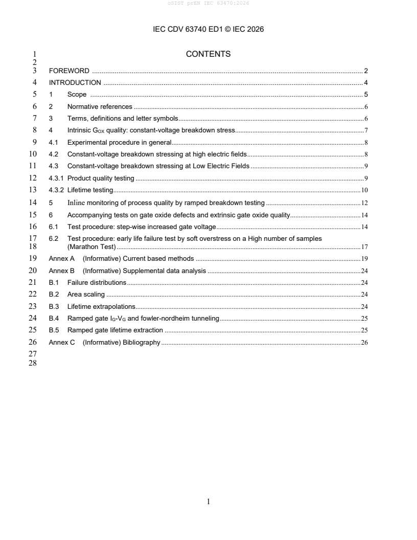
1 CONTENTS
3 FOREWORD . 2
4 INTRODUCTION . 4
5 1 Scope . 5
6 2 Normative references . 6
7 3 Terms, definitions and letter symbols . 6
8 4 Intrinsic G quality: constant-voltage breakdown stress. 7
OX
9 4.1 Experimental procedure in general . 8
10 4.2 Constant-voltage breakdown stressing at high electric fields . 8
11 4.3 Constant-voltage breakdown stressing at Low Electric Fields . 9
12 4.3.1 Product quality testing . 9
13 4.3.2 Lifetime testing. 10
14 5 Inline monitoring of process quality by ramped breakdown testing . 12
15 6 Accompanying tests on gate oxide defects and extrinsic gate oxide quality. 14
16 6.1 Test procedure: step-wise increased gate voltage . 14
17 6.2 Test procedure: early life failure test by soft overstress on a High number of samples
18 (Marathon Test) . 17
19 Annex A (Informative) Current based methods . 19
20 Annex B (Informative) Supplemental data analysis . 24
21 B.1 Failure distributions . 24
22 B.2 Area scaling . 24
23 B.3 Lifetime extrapolations. 24
24 B.4 Ramped gate IG-VG and fowler-nordheim tunneling . 25
25 B.5 Ramped gate lifetime extraction . 25
26 Annex C (Informative) Bibliography . 26
IEC CDV 63740 ED1 © IEC 2026
29 INTERNATIONAL ELECTROTECHNICAL COMMISSION
31 GUIDELINE FOR GATE OXIDE RELIABILITY AND ROBUSTNESS EVALUATION
32 PROCEDURES FOR SILICON CARBIDE POWER MOSFETS
34 FOREWORD
36 1) The International Electrotechnical Commission (IEC) is a worldwide organization for standardization comprising
37 all national electrotechnical committees (IEC National Committees). The object of IEC is to promote
38 international co-operation on all questions concerning standardization in the electrical and electronic fields.
39 To this end and in addition to other activities, IEC publishes International Standards, Technical Specifications,
40 Technical Reports, Publicly Available Specifications (PAS) and Guides (hereafter referred to as “IEC
41 Publication(s)”). Their preparation is entrusted to technical committees; any IEC National Committee interested
42 in the subject dealt with may participate in this preparatory work. International, governmental and non- governmental
43 organizations liaising with the IEC also participate in this preparation. IEC collaborates closely with the
44 International Organization for Standardization (ISO) in accordance with conditions determined by agreement
45 between the two organizations.
46 2) The formal decisions or agreements of IEC on technical matters express, as nearly as possible, an international
47 consensus of opinion on the relevant subjects since each technical committee has representation from all
48 interested IEC National Committees.
49 3) IEC Publications have the form of recommendations for international use and are accepted by IEC National
50 Committees in that sense. While all reasonable efforts are made to ensure that the technical content of IEC
51 Publications is accurate, IEC cannot be held responsible for the way in which they are used or for any
52 misinterpretation by any end user.
53 4) In order to promote international uniformity, IEC National Committees undertake to apply IEC Publications
54 transparently to the maximum extent possible in their national and regional publications. Any divergence
55 between any IEC Publication and the corresponding national or regional publication shall be clearly indicated
56 in the latter.
57 5) IEC itself does not provide any attestation of conformity. Independent certification bodies provide conformity
58 assessment services and, in some areas, access to IEC marks of conformity. IEC is not responsible for any
59 services carried out by independent certification bodies.
60 6) All users should ensure that they have the latest edition of this publication.
61 7) No liability shall attach to IEC or its directors, employees, servants or agents including individual experts and
62 members of its technical committees and IEC National Committees for any personal injury, property damage or
63 other damage of any nature whatsoever, whether direct or indirect, or for costs (including legal fees) and
64 expenses arising out of the publication, use of, or reliance upon, this IEC Publication or any other IEC
65 Publications.
66 8) Attention is drawn to the Normative references cited in this publication. Use of the referenced publications is
67 indispensable for the correct application of this publication.
68 9) Attention is drawn to the possibility that some of the elements of this IEC Publication may be the subject of
69 patent rights. IEC shall not be held responsible for identifying any or all such patent rights.
IEC CDV 63740 ED1 © IEC 2026
71 International Standard IEC XXXXX has been prepared by subcommittee XX: TITLE, of IEC
72 technical committee XX:XXX.
73 This document is based upon JEDEC JEP194 and was submitted as a Fast-Track document. It
74 is used with permission of the copyright holder, JEDEC Solid State Technology Association.
75 The text of this International Standard is based on the following documents:
FDIS Report on voting
XX/XX/FDIS XX/XX/RVD
78 Full information on the voting for the approval of this International Standard can be found
79 in the report on voting indicated in the above table.
80 This document has been drafted in accordance with the ISO/IEC Directives, Part 2.
81 The committee has decided that the contents of this document will remain unchanged until the
82 stability date indicated on the IEC website under "http://webstore.iec.ch" in the data related to
83 the specific document. At this date, the document will be
84 • reconfirmed,
85 • withdrawn,
86 • replaced by a revised edition, or
87 • amended.
The National Committees are requested to note that for this document the stability date
is 20XX.
THIS TEXT IS INCLUDED FOR THE INFORMATION OF THE NATIONAL COMMITTEES AND WILL BE
DELETED AT THE PUBLICATION STAGE.
IEC CDV 63740 ED1 © IEC 2026
92 INTRODUCTION
94 (From JEDEC Board Ballot JCB-22-61, formulated under the cognizance of the JC-70.2
95 Subcommittee on SiC Power Electronic Conversion Semiconductor Standards.)
97 This document was formulated by JEDEC JC-70.2 SiC Power Electronics Conversion
98 Semiconductor Standards subcommittee consisting of worldwide industry experts from various
99 power semiconductor, power supply and test equipment manufacturing companies.
101 This document has the purpose of laying out generally acceptable practices for testing gate oxide
102 reliability of silicon carbide (SiC) based power devices having a gate dielectric region involved
103 in turning devices on and off. This typically refers to metal-oxide-semiconductor (MOS) devices
104 such as capacitors, field-effect transistors (MOSFETs), or insulated-gate bipolar transistors
105 (IGBTs). All presented examples are from MOS gated SiC devices. Specifically covered is time-
106 dependent dielectric breakdown (TDDB) testing, with either constant-voltage stress (CVS),
107 constant-current stress (CCS) or ramped voltage stress (RVS) / ramped current stress (RCS) for
108 ramped breakdown (RBD) tests.
110 An issue related particularly to SiC substrates is their high defect density; which has been rapidly
111 decreasing over time as substrate quality improves, but remains orders of magnitude higher than
112 for silicon substrates. This, and the resulting high interface trap levels present at SiO /SiC
113 interfaces, has in the past interfered with the understanding of the intrinsic properties of SiO on
114 SiC. Thus, in the testing guidelines presented here, the intrinsic properties of the oxides on SiC
115 are themselves important to demonstrate/determine. Extrinsic failures can often be related to
116 intrinsic material defects in the SiC wafer material, or to processing issues, and any mathematical
117 treatment of extrinsic defects is beyond the scope of this document. For detailed analysis of early
118 fail populations (See JESD74A). Of course, the testing recommended here is to allow
119 determination of the intrinsic and extrinsic populations, specifically through analysis of the
120 failure distributions. However, the reasons for extrinsic failures, and means to eliminate them,
121 are not addressed here, but helpful experimental procedures to analyze extrinsic failures will be
122 described.
IEC CDV 63740 ED1 © IEC 2026
124 GUIDELINE FOR GATE OXIDE RELIABILITY AND ROBUSTNESS EVALUATION
125 PROCEDURES FOR SILICON CARBIDE POWER MOSFETS
127 1 Scope
129 This document has two purposes; the first is presenting guidelines for the gate dielectric lifetime extraction
130 and wear-out of MOS devices on silicon carbide substrates ("intrinsic behavior"). Specifically, it is
131 designed for MOS devices (capacitors or transistors) where oxide thickness (tox) >> 10 nm. Therefore, ‘soft’
132 breakdown behavior is not expected to be observed, and oxide breakdown occurs instantaneously as a ‘hard’
133 breakdown event. Thus, issues relating specifically to thin oxides and soft breakdown are not addressed
134 here. The second purpose is presenting guidelines for the measurement of gate dielectric breakdown, which
135 are assumed to be defect related and occur much earlier than the wear out (“extrinsic behavior”). Although
136 almost all data available in literature is on SiO as a gate dielectric, the procedures outlined in this document
137 apply to any dielectric layer. In case of a gate stack of different dielectrics, special care has to be taken
138 when calculating the field distribution across the dielectric stack. This is not covered by this document.
140 MOS devices such as MOSFETs and IGBTs are designed to be operated at a fixed gate voltage (V ) level
GS
141 in the ON-state. As-such, oxide lifetime under controlled gate bias conditions is most appropriate for oxide
142 lifetime extraction. On the other hand, charge to breakdown measurements or constant current stress can
143 provide an alternative way to estimate lifetime, provided some conditions are fulfilled. Practical tests, which
144 give oxide lifetime-related information, are (usually on-wafer and/or packaged devices):
145 • Constant-voltage stress (CVS) time-dependent dielectric-breakdown (TDDB) testing over short and
146 relatively long time periods.
147 • Ramped-voltage stress (RVS) or ramped breakdown (RBD) approaches in which data for many samples
148 can be obtained quickly. A voltage ramp is typically used for this test (V-Ramp), although a current,
149 or current density ramp (J-Ramp), can be performed as well.
150 • Constant current stress (CCS) time dependent dielectric breakdown testing for low and high current
151 densities.
152 It should be pointed out that all discussed tests provoke so-called hard-fails. This means that the device is
153 typically “short” after the failure. “Soft” gate oxide failures (only a slight increase of the gate leakage
154 current) as well as fails by parameter shifts were not expected in the typical gate oxide thickness range of
155 SiC-based power-semiconductors. Furthermore, parameters like VTH are typically shifting in such tests, but
156 this is not a topic of interest in the evaluation of the tests.
158 Testing of gate oxide breakdown under accelerated bias, current or temperature conditions does not replace
159 traditional qualification tests such as high-temperature gate bias (HTGB) testing called for in, for example,
160 JESD22-A108F. This document is not meant to define acceptable lifetime limits, or proscribe acceptable
161 use conditions; that is up to the device manufacturers and users.
IEC CDV 63740 ED1 © IEC 2026
163 2 Normative references
165 This guideline is meant to point out specific practices that may be applicable when testing gate oxide
166 reliability for SiC-based power MOS devices. Practices proscribed in the following documents are to be
167 followed, except where they are specifically modified in this present document:
169 The following normative documents contain provisions that, through reference in this text, constitute
170 provisions of this standard. For dated references, subsequent amendments to, or revisions of, any of these
171 publications do not apply. However, parties to agreements based on this standard are encouraged to
172 investigate the possibility of applying the most recent editions of the normative documents indicated
173 below. For undated references, the latest edition of the normative document referred to applies.
174 JEP001A, Foundry Process Qualification Guidelines (2014).
175 JEP122H, Failure Mechanisms and Models for Silicon Semiconductor Devices (2016).
176 JESD35-A, Procedure for the Wafer-Level Testing of Thin Dielectrics (2001).
177 JESD35-2, Test Criteria for the Wafer-Level Testing of Thin Dielectrics (1996).
178 JESD47J.01, Stress-Test-Driven Qualification of Integrated Circuits (2017).
179 JESD91B, Method for Developing Acceleration Models for Electronic Device Failure Mechanisms
180 (2022).
181 JESD92, Procedure for Characterizing Time-Dependent Dielectric Breakdown of Ultra-Thin Gate
182 Dielectrics (2003).
185 3 Terms and definitions
187 For the purposes of this publication, the following terms and definitions apply.
189 Terms in order of relevance:
191 TDDB: Time-dependent dielectric breakdown; most properly applies to conditions where all parameters
192 are fixed except for time, but it is often applied to breakdown testing when other parameters are also varied
193 (such as voltage or current) besides time.
195 CVS: Constant voltage stress; this is the typical TDDB condition, sometimes referred to as CV-TDDB to
196 differentiate from ramped tests.
198 CCS: Constant current stress; is a TDDB condition in which the current density is kept constant during the
199 duration of the stress.
201 RBD: Ramped breakdown; if voltage is ramped, it may be referred to as Ramped Voltage Stress (RVS),
202 or V-Ramp; if current (or current density) is ramped, it is referred to as a Ramped Current Stress (RCS) or
203 J-Ramp test.
IEC CDV 63740 ED1 © IEC 2026
206 Defined variables in order of relevance:
208 t : Time to breakdown (often units of seconds, or hours). The value t refers to the failure time for 63%
BD 63
209 of the devices (the Weibull alpha ), t refers to the time, at which 50% of the population fails (for
210 lognormal distributions), etc.
212 t : Oxide (or dielectric) thickness, measured electrically, optically, or physically.
ox
214 V : Voltage drop across oxide [V]
ox
216 E : Oxide field [V/cm], V /t . V should be corrected for capacitor flatband voltage (V ) if V is
ox ox ox ox fb fb
217 significant compared to V .
BD
219 V : Oxide film breakdown voltage [V]
BD
221 Q : Charge to breakdown; t x J for a CCS experiment. J is the current density during stress, t
BD fail dens dens fail
222 is the time to failure.
225 4 Intrinsic G quality: constant-voltage breakdown stress
OX
227 For SiC power MOS-based devices (MOS capacitors, MOSFETs, and IGBTs, for example), constant-
228 voltage time-dependent dielectric breakdown (TDDB) testing should in most regards be consistent with
229 the approaches established for silicon-based MOS devices in JEP001A for process qualifications, in
230 JESD47J.01 for part qualifications, or as in JESD92 for characterizing gate oxide reliability and
231 predicting lifetime, and JEP122H for mathematical description (models). Generally important aspects of
232 testing are mentioned herein as guidelines for SiC power device testing.
234 JESD47J.01 recommends that either TDDB data or charge-to-breakdown data be available when new
235 wafer fabrication or dielectric materials are utilized in a device family. General testing guidelines follow
236 from JEP001 and JESD92. Because MOS devices are operated with a constant gate bias in the ON-state,
237 constant voltage TDDB testing (time dependent dielectric breakdown, time-to-breakdown) is
238 recommended for failure distribution and lifetime evaluation rather than constant-current testing
239 (charge-to-breakdown). Although capacitor structures fabricated with the same processing as MOS
240 transistors are allowed in other existing JEDEC documents, we recommend the testing of the actual
241 product (i.e., transistors) where possible with positive polarity at the gate terminal (use case of the
242 devices). Also voltage stress with negative polarity at the gate terminal should be considered if the
243 devices are specified to have a negative gate voltage during turn-off.
245 If capacitors are used, they should be biased in accumulation, corresponding to the bias polarity used for
246 the actual product. We want to point out that capacitor structures are less complex than transistors (in
247 planar as well as in trench concepts) which may result in different, perhaps too optimistic experimental
248 results.
IEC CDV 63740 ED1 © IEC 2026
250 The tested devices should be of large enough area to fairly represent product devices. We recommend
251 measuring the biggest device in a device family which is expected to have the lowest lifetime in TDDB
252 experiments due to the expected higher number of defects present in such devices, and to carry out
253 investigations on area scaling whenever necessary.
255 4.1 Experimental procedure in general
257 As a prerequisite, comparable groups of devices (same product type, same specification, standard
258 production) should be chosen. Continuous monitoring of gate leakage (for CVS) or of voltage (for CCS)
259 across the gate dielectric is the preferred way to determine failure time. Known good devices are selected
260 for the test. The time to breakdown for each device at the V stressing value (constant voltage stress).
GS
261 The failure criteria must be consistent; typically a leakage current value or a current increase rate (or a
262 drop in V if V is being monitored). Issues mentioned in JESD92 Annex A should be considered
GS GS
263 regarding the measurement and instrumentation requirements. The number of devices tested per stress
264 condition should be at least 25 devices.
266 4.2 Constant-voltage breakdown stressing at high electric fields
268 At high electrical fields the failure mechanism is expected to change during the experiment, and the
269 observed parameters are not valid for lifetime extrapolation. Such experiments can be performed either on
270 wafer material or with discrete packaged parts. The derived failure distribution can typically be separated
271 in an intrinsic and an extrinsic part and allows conclusions on electrical defect density. The observed -
272 values may not be representative of low-field behavior due to additional failure mechanisms which
273 become active at high fields, but the results of high-field testing are sufficient to compare different
274 process variations. Also the t /t -values can be used for process comparisons. Contrary, the observed
63 50
275 −values are typically very high and an extrapolation to lower electrical fields would likely lead to wrong
276 results.
278 At high electrical fields, failure of the dielectric is due to positive charge trapping. Typically this occurs
o
279 for E >8 MV/cm at room temperature, and E >9 MV/cm at T = 175 C. A practical way to assess if one
ox ox
280 is in the positive charge trapping regime, is by inspecting the I -t (for constant voltage stress) or V -t (for
g g
281 constant current stress) curves. If I increases as a function of stress time (or V decreases), one is under
g g
282 the “high field” stress condition.
IEC CDV 63740 ED1 © IEC 2026
285 4.3 Constant-voltage breakdown stressing at low electric fields
287 Parameters of such experiments (described by the t /t , , ) are suited for lifetime extrapolation towards
63 50
288 typical use fields. Such experiments are typically carried out by testing of discrete packaged parts in an
289 oven because this setup allows long stress times (hundreds of hours, even 1000 hrs or 2000 hrs). The
290 derived failure distribution can also typically be separated in an intrinsic and an extrinsic part and allows
291 conclusions on electrical defect density.
293 At low electrical fields, failure of the dielectric is due to negative charge trapping. Typically this occurs
o
294 for E <8 MV/cm at room temperature, and E <9 MV/cm at T = 175 C. A practical way to assess if one
ox ox
295 is in the negative charge trapping regime, is by inspecting the I -t (for constant voltage stress) or V -t (for
g g
296 constant current stress) curves. If I decreases as a function of stress time (or V increases), one is under
g g
297 the “low field” stress condition. An example is given in Figure 10.
299 4.3.1 Product quality testing
301 For a representative product family, at least 3 representative groups of parts (typically ≥25 or more
302 parts/group) should be stressed at different V values greater than V (use), and held until
GS(stress) GS
303 approximately 63% of the population fails. Then a field acceleration parameter () can be calculated for
304 lifetime determination at the use voltage. Ideally all parts should be taken to failure, or at least one of
305 the 3 populations (for a complete failure distribution determination). If V values have been
GS
306 appropriately chosen, all failures should occur within the ranges of hours to a thousand hours. If all parts
307 in all 3 populations fail in less than 10 hours, then the voltage levels chosen are too high, and this may
308 not properly provide true lifetime extrapolation. Ideally these tests are performed at the device
309 maximum rated use temperature, as it is known that failure rates of SiO (and oxide dielectrics in
310 general) increase with increasing temperature. It is recommended to have all parts under test held in an
311 oven for temperature uniformity.
313 A Weibull plot of percent failure versus time will give the Weibull slope beta () for each population,
314 and the measured t is the Weibull scale parameter alpha (). For product quality testing, Weibull slope
315 value , and projected lifetime for the t or t failure percentages at the V (use) value using the linear
63 50 GS
316 field E-model, are recommended as quality metrics. Since the intrinsic Weibull slope β is a
317 characteristic of the dielectric under stress, it should be independent of the stress condition and hence all
318 failure data should be fitted with one intrinsic Weibull slope (and not a different Weibull slope per
319 individual stress condition).
n
321 As per the field acceleration model, different models exist in literature (E-model, 1/E model, V model). It
322 is recommended to use the most conservative model (E-model) unless that data unambiguously points to
323 another field acceleration model.
IEC CDV 63740 ED1 © IEC 2026
326 4.3.2 Lifetime testing
328 For a complete intrinsic lifetime determination, parts should be tested at various temperatures, such as
rd
329 room temperature (25°C) and the maximum allowed operation temperature, and preferably a 3
330 temperature (either intermediate or somewhat higher than the maximum allowed use temperature). The
331 maximum allowed temperature has to be tested in any case. As mentioned in the previous subclause, at
332 least 3 groups of parts (with typically ≥25 or more parts/group) should be stressed at V values greater
GS
333 than V (use), and held until at least 63% of the population fails, for each temperature. Outliers
GS
334 (extrinsics; i.e., measurement values significantly deviating from the intrinsic Weibull data fit) should be
335 excluded. To determine if a part belongs to the intrinsic distribution or not, 95% confidence levels can be
336 used.
338 Then a temperature-dependent field acceleration parameter or an apparent activation energy can be
339 calculated, to allow lifetime determination at the use voltage for a range of temperatures. Ideally all parts
340 should be taken to failure for at least one of the populations at each temperature. If V values have been
GS
341 appropriately chosen, all failures should occur within the ranges of hours to a thousand hours. If all parts
342 in all 3 populations fail within, or close to, 10 hours, then the voltage levels chosen are too high, and this
343 may not properly provide true lifetime extrapolation. Parts for package level tests are held in an oven to
344 maintain uniform temperature ambient. The same can be achieved for wafer level tests via a thermo
345 chuck.
347 A Weibull plot of percent failure versus time will give the Weibull slope for each population, and the
348 measured t is the Weibull scale parameter . From the t time for each of the 3 populations (or another
63 63
349 representative time such as t50), a plot of ln(tBD) versus VGS can be used to extrapolate lifetime to the use
350 V value (for at least 3 populations measured at a fixed temperature). This type of extrapolation
GS
351 presumes that the linear field model (E-model) is the appropriate model to determine lifetime. Although
352 some debates exist concerning appropriate lifetime modeling, it is recommended to use the “Linear-E-
353 model” as it gives a slightly more conservative lifetime prediction than other approaches and is simple to
354 apply. This is especially the case for devices with thick gate oxide layers (>20 nm). Power law
355 extrapolation or other mathematical approaches should only be used if they could be experimentally
356 verified; in case of their use the lifetime extrapolation method should be clearly stated.
358 When measurements are performed at multiple temperatures, the representative t for each population
BD
359 (t or t ) at the given temperature can be plotted versus inverse temperature, and the effect of
63 50
360 temperature on lifetime will be shown. The effects of temperature can be lumped into the field
361 acceleration parameter, or listed as an apparent activation energy, depending on the mathematical
362 approach used (See subclause B.3).
364 In summary, CVS TDDB data is best displayed by:
365 1) Weibull plots showing the failure distribution at a given temperature and V condition, with the
GS
366 Weibull slope calculated by fitting the majority of the distribution (this focusses on the intrinsic
367 population).
368 2) Lifetime plots extrapolating the failure time (t , t , or other representative failure percentile such as
63 50
369 t ) to the use voltage, preferably plots of ln(t ) versus V fit using a straight line in the case of the
1 BD GS
370 E-model to obtain failure rates at the V (use) value. Other lifetime extrapolation methods can be
GS
371 used, as long as the approach is clearly defined and experimentally verified.
IEC CDV 63740 ED1 © IEC 2026
374 NOTE 1 This example TDDB Weibull failure distribution is for parts held at one stress condition including fit line
375 and 95% confidence level (left), and failure time extrapolation for 3 groups of stressed parts, using a straight line to
376 fit the 63%, 1%, and 1 ppm failure populations (right). From the lifetime plot, estimated lifetime at any given V
GS
377 value can be obtained (at that measurement temperature).
379 NOTE 2 Exemplarily, a potential device specification of 15 V/20 y was added in the figure on the right side.
381 Figure 1 — TDDB Weibull Failure Distribution
IEC CDV 63740 ED1 © IEC 2026
384 5 Inline monitoring of Process quality by ramped breakdown testing
386 To get a fast estimation of the gate oxide defect density, one can use ramped voltage or ramped current
387 approaches (termed V-Ramp and J-Ramp in JESD35A). These tests are typically carried out in a way that
388 the tested devices are stressed to failure/breakdown (end-of-life test). Both methods are faster and simpler
389 than traditional TDDB measurements. As such, they can be very useful for process control monitoring. In
390 principle they can also be used for lifetime extrapolations (See [5], [6] and subclause B.5), although some
391 debate remains as to whether it gives predictions equivalent to TDDB testing. Thus, TDDB is the
392 recommended test for lifetime evaluation, but the V-ramp technique is probably a more useful technique
393 for quickly monitoring oxide quality with high statistics.
395 Ramped breakdown testing is usually performed (inline, after wafer processing) on a (semi-) automatic
396 probe station with a heated chuck, such that testing of many dies on a wafer can be automated. Typically
397 a pretest of I is performed at V (use) before the voltage is ramped from a level below V (use) until the
GS GS GS
398 breakdown occurs. As in TDDB, breakdown is defined by reaching a given current level or a current
399 increase above a certain rate. It is desirable to maintain the complete set of I -V data in order to plot the
g g
400 data and extract Fowler-Nordheim dielectric/SiC barrier height for the product being measured, and to
401 document how the breakdown event proceeds.
403 The voltage step size of the ramp should be small enough to obtain a V value allowing good resolution
BD
404 of the failure voltage for each part, such as a voltage step which is <1% of the V for that product. The
BD
405 total ramp rate should be moderate and within the capability of the measurement setup. It should not be
406 too fast (e.g., steps in the low ms or µs-range) as not to reach significantly higher VBD values as in the
407 TDDB test thereby invoking other (high-field) failure mechanisms (observing the same failure
408 mechanism as measured in TDDB is the goal of this test). The ramp rate should be such that t is at
BD
409 minimum greater than about 10 seconds for a given ramp rate, to not compromise accuracy and
410 repeatability.
412 For process quality monitoring, testing of a (randomly selected) population of ~100 parts (die, or on-
413 wafer) is typically sufficient. If failure probabilities in the 1% range or lower are of interest, it is
414 recommended to measure much more than 100 parts. This is the principal reason to use the V-Ramp
415 approach, to measure large numbers of samples quickly. For this, a single ramp rate (giving a reasonable
416 failure time resolution) and a single temperature (ideally the device rated temperature) can be used.
418 To test gate oxide defect density that is independent of device structure (e.g., quality of the oxidation or
419 deposition process), large MOS capacitors are very appropriate to use. From this test, a failure distribution
420 plot on a Weibull scale versus the VBD gives the pertinent information regarding the oxide properties of
421 the population tested (Figure 2). Here the Weibull parameter gives the breakdown voltage 63% failure
422 quantile, and the slope is a measure of oxide quality (but is not the same as the Weibull slope for TDDB
423 measurements versus time).
IEC CDV 63740 ED1 © IEC 2026
-1
-2
-3
-4
-5
-6
-7
10 20 30 40 50
V (fail) [V]
gs
427 NOTE This is an example of ramped breakdown failure points (Vgs at failure) for a group of 250 large area
428 capacitors taken to breakdown.
430 Figure 2 — Ramped Breakdown Failure Distribution for Large-Area Capacitors
432 The defect density level of the process can also be analyzed. For this purpose, fully processed devices
433 need to be used, and the sampling has to be chosen adequately. Extrinsic devices can be observed as
434 devices with VBD breakdown values deviating from the Weibull failure distribution (See JESD35A,
435 subclause A.2). It is expected that they are the result of defects in the gate oxide or local oxide thinning.
436 For further root cause analysis, methods of the physical failure analysis can be used.
438 The transition from extrinsic to intrinsic data points within a failure distribution is indicated by an
439 inclination point which discriminates between the measured devices with an intrinsic and an extrinsic
440 failure mechanism. Even if it is quite straightforward to estimate the total (extrinsic) defect density, it is
441 much harder to determine whether an extrinsic defect (that fails at a somewhat lower V -value) is
BD
442 actually critical for the application, i.e., if the affected device would fail during the aspired device lifetime
443 or not. Additional analysis techniques and other test setups have to be considered for that.
ln(-ln(1-F))
IEC CDV 63740 ED1 © IEC 2026
446 6 Accompanying tests on gate oxide defects and extrinsic gate oxide quality
448 In this chapter, methods are described to analyze and compare the gate oxide properties of different SiC
449 MOSFET groups, e.g., from different technology nodes or different manufacturers.
451 As a prerequisite SiC MOSFETs have to be used which are representative for the typical outgoing quality
452 of the particular manufacturer, and have been exposed to all prescribed tests by the manufacturer (optical
453 inline inspections, electrical tests and screening, burn-in etc.).
455 6.1 Test procedure: step-wise increased gate voltage
457 In this subclause, a test procedure to compare extrinsic and intrinsic gate oxide properties of different SiC
458 MOSFET devices will be discussed. The test is based on a stepped gate voltage sequence, which is
459 performed at elevated temperature [2], [4]. To perform the test, only some basic datasheet values need to
460 be known:
461 • The recommended gate use voltage (𝑉 ), the maximum allowed gate use voltage (𝑉 ), and
𝐺,𝑢𝑠𝑒 𝐺,𝑚𝑎𝑥
462 the recommended use temperature (𝑇 ).
𝑢𝑠𝑒
463 • An ensemble of SiC MOSFET devices, e.g., 100 parts, is pre-characterized at room temperature. For
464 instance, gate integrity is measured.
𝑉
𝐺𝑆
𝑉
𝐺𝑆,𝑖𝑛𝑡𝑟
𝑇𝑒𝑚𝑝 = 𝑇
𝑢𝑠𝑒
𝑉 + 4𝑉
𝐺𝑆,𝑚𝑎𝑥
𝑉 + 2𝑉
𝐺𝑆,𝑚𝑎𝑥
𝑉
𝐺𝑆,𝑚𝑎𝑥
𝑉
𝐺𝑆,𝑟𝑒𝑐
. . . .
𝑡
𝑠𝑡𝑟
𝑡
467 Figure 3 — Proposed Gate Voltage Step Test Sequence
IEC CDV 63740 ED1 © IEC 2026
468 Referring to Figure 3, before and after each stress sequence, the gate integrity of each chip is checked via
469 an IGSS (gate-source leakage) test. The procedure is an end-of-life test.
471 In a first stress step, all devices are stressed at the temperature 𝑇 , e.g., 150 °C, for a time 𝑡 at the
𝑢𝑠𝑒 𝑠𝑡𝑟
472 recommended gate use voltage 𝑉 . After stress, all devices are checked for IGSS (gate-source leakage
𝐺,𝑢𝑠𝑒
473 current) failures. An appropriate stress time 𝑡 could be 18h so that one cycle of stress and measurement
𝑠𝑡𝑟
474 could be carried out in 1 day. Also, longer stress times like 168 hrs could be chosen. Devices which failed
475 during step 1 are counted and removed from the distribution. The second stress step is performed in the
476 same way but at the maximum allowed use voltage 𝑉 . Devices which failed during step 2 are again
𝐺,𝑚𝑎𝑥
477 counted and removed from the distribution. The test is continued in this way with gradually increasing
478 stress voltage, e.g., by +2 V after each stress step, until all devices have failed. Also, other voltage step
479 sizes could be chosen, but it is advised to use roughly 20-30 equidistant steps between 𝑉 and V
BD
𝐺,𝑢𝑠𝑒
480 (V should be determined beforehand in a fast voltage ramp experiment).
BD
482 At the end of the test, the failed devices after each stress step are analyzed in a Weibull plot.
484 Experimentally, the CDF can be determined using Bernard’s approximation:
𝑖−0.3
485 𝐹 = (1)
𝑖
𝑁+0.4
486 where 𝑖 is a running index indicating the number of failed devices and 𝑁 is the total number of tested
487 devices. The y-axis of the Weibull plot is calculated by linearization of the cumulative density function
488 (CDF)
𝑡
𝑢𝑠𝑒
489 𝑙𝑛(− 𝑙𝑛(1 − 𝐹 )) = 𝛽 ∙ 𝑙𝑛 ( ) (2)
𝑖
𝜏
490 Using the linear E-model, the life time (typically the x-axis of the Weibull plot) can be expressed as a
′
491 function of the difference 𝑉 − 𝑉 for an extrinsic spot with an electrical oxide thickness 𝑑
𝐺,𝑠𝑡𝑟 𝐺,𝑢𝑠𝑒 𝑜𝑥
𝛾
492 𝑡 = 𝑡 𝑒𝑥𝑝 ( (𝑉 − 𝑉 )) (3)
𝑢𝑠𝑒 𝑠𝑡𝑟 ′ 𝐺,𝑠𝑡𝑟 𝐺,𝑢𝑠𝑒
𝑑
𝑜𝑥
′
493 𝑑 is related to the stress time (𝑡 ) and the stress voltage (𝑉 ) at which the defective device fails.
𝑜𝑥 𝑠𝑡𝑟 𝐺,𝑠𝑡𝑟
1ℎ
494 𝐸 is the value for the electrical field at which a typical intrinsic breakdown occurs after 1 hour:
𝐵𝐷
𝑡 𝑉
𝑠𝑡𝑟 𝐺,𝑢𝑠𝑒
1ℎ
( ) ( )
495 𝑡 = 𝑡 𝑒𝑥𝑝 ( 𝛾𝐸 − 𝑙𝑛 ( ) 1 − ) (4)
𝑢𝑠𝑒 𝑠𝑡𝑟 𝐵𝐷
3600 𝑉
𝐺,𝑠𝑡𝑟
𝑡 𝑡 𝑉
𝑠𝑡𝑟 1ℎ 𝑠𝑡𝑟 𝐺,𝑢𝑠𝑒
497 𝑙𝑛 (− 𝑙𝑛(1 − 𝐹 )) = 𝛽 [𝑙𝑛 ( )] + 𝛽 (𝛾𝐸 − 𝑙𝑛 ( )) (1 − ) (5)
𝑖
𝐵𝐷
𝜏 3600 𝑉
𝐺,𝑠𝑡𝑟
IEC CDV 63740 ED1 © IEC 2026
499 In the double logarithmic ordinate (y-axis) representation, the Weibull distribution described in the
500 equation above shows a linear increase over time if one minus the ratio of use and stress voltage is chosen
501 as the abscissa (x-axis). Note that the slope depends only on material parameters and on the stress cycle
...